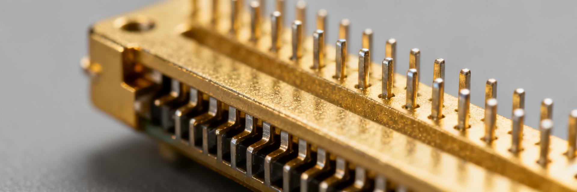
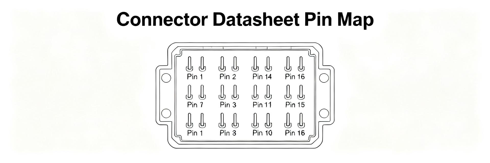
31068-1010 Datasheet: Pinout, Current and Voltage Facts
Per typical datasheet figures, the 31068-1010 is a 4-position rectangular receptacle with a 2.54 mm (0.100 in) pitch, rated typically for 9–11 A per contact, and specified for operation from −40 °C to +100 °C. Contacts are commonly plated with a corrosion-resistant finish and the housing uses a high‑temperature insulating polymer. This quick-reference compiles the critical numeric facts engineers need to speed design checks, prevent derating errors and ensure correct pin wiring during harness and PCB integration. The value proposition is immediate: a single‑page synthesis of pinout conventions, mechanical limits, electrical ratings and assembly checks so designers avoid last‑minute redesigns. For definitive verification always cross‑check against the official datasheet and manufacturer documentation before release to production. 31068-1010 Connector Overview and Key Specifications (Background) Quick Specs Table Positions 4-Position Receptacle Pitch 2.54 mm (0.100 in) Current Rating 9 – 11 A per contact Temp Range −40 °C to +100 °C Mechanical form factor & pin count The 31068-1010 is a 4‑position receptacle designed for cable/harness use with a 2.54 mm (0.100 in) centerline and keyed polarization to prevent reverse mating. Typical dimensions to note are pitch 2.54 mm, overall housing length proportional to four positions plus retention features, and a female/gendered receptacle intended for crimped contacts. A compact table in the datasheet shows positions, pitch, gender and recommended housing material—reference the official datasheet for exact mechanical drawings. Environmental & material limits Datasheet entries typically list operating temperature from −40 °C to +100 °C and specify a high‑temperature thermoplastic insulation. Contact plating is usually tinned over a copper alloy; gold plating may be specified for high‑reliability variants. Engineers should flag limits on humidity and thermal cycling found in the datasheet, as ingress or sustained elevated ambient temperatures are common field failure drivers when margins are not observed. 31068-1010 Pinout, Pin Functions and Wiring Notes (Data analysis) Pin numbering convention & typical wiring map Pin numbering follows a sequential convention: Pin 1 at the keyed corner, then Pins 2–4 across the row. A common wiring map for power harnesses maps Pin 1 → V+, Pin 2 → V+, Pin 3 → GND, Pin 4 → GND when paralleling for current sharing. Recommended wire gauges depend on current: for sustained 8–11 A, use wire in the 16–18 AWG range; the datasheet pinout diagram should be confirmed against your CAD symbol and assembly drawings before routing. Crimp/contact interface and mating notes The connector accepts discrete crimp contacts; datasheet callouts include insertion depth, retention force and contact orientation. Best practice: verify correct crimp quality (conductor and insulation indent), ensure polarization features seat fully and use strain relief to prevent conductor pull‑out. For high currents, consider ferrules on stranded conductors and route harnesses to minimize bundle heating and stress on crimps. Electrical Data Deep-Dive: Current Rating, Voltage Limits and Thermal Considerations Current per contact & Derating Typical rated current is listed at about 9–11 A per contact under datasheet test conditions, which usually assume a given ambient temperature and a maximum contact temperature rise. Derating is required for higher ambient temperatures or grouped conductors: for each 10 °C rise in ambient beyond the baseline, reduce allowable current per contact according to the manufacturer’s derating curve. Voltage & Insulation Voltage rating in similar housings is often in the low‑voltage class (tens to low hundreds of volts) with insulation resistance in the gigaohm range when new. Checklist: confirm maximum working voltage, insulation resistance, and minimum creepage distance in the official datasheet. Design & Assembly Guide: How to Use the Datasheet PCB / harness integration checklist Verify the pinout against your schematic. Confirm current and voltage ratings. Select wire gauge and crimp contact compatible with the housing. Provision strain relief. On the PCB, match pad spacing to 2.54 mm pitch and include mechanical retention. Soldering/crimping and quality verification steps Adopt a validated crimp process: crimp height and pull‑force checks, visual inspection for conductor extrusion, and sample continuity and contact resistance testing. Acceptable contact resistance typically falls in the milliohm range; higher than expected values indicate poor crimps or contamination. Capture lot and test data on the BOM and assembly drawings for traceability and production QA. Real-World Example: Integrating 31068-1010 into a Power Harness Example scenario: A 12 V distribution harness carrying up to 8 A per line. Using the datasheet’s 9–11 A typical rating, the designer selects 18 AWG stranded conductors, adds parallel wiring on V+ pins for margin, and spaces connectors to avoid heat accumulation. Decision points: if continuous current exceeds the lower bound of the rating, either parallel contacts or select a higher‑rated connector family based on datasheet tables. Validation & lab checklist Prototype tests include current cycling at target load for several hours, thermal imaging to confirm contact temperature within datasheet limits, and vibration to validate retention. Pass criteria derive from datasheet maximum contact temperature and mechanical retention forces; failures should trigger rework of crimp process, harness routing or connector choice. Testing, Troubleshooting and Final Checklist Common Failure Modes Loose crimps / High resistance Miswiring / Pin mapping errors Overheating under sustained load Pre-production Checklist Confirm Part Number vs Datasheet Verify Pinout in CAD Verify Derating Margins Summary Engineers should retain three critical datapoints from this guide: clear verification of the pinout in CAD and harness drawings, strict adherence to current/voltage limits with appropriate derating for ambient and bundling, and disciplined crimp/assembly QA to avoid field failures. Use the datasheet as the single source of truth for mechanical drawings, electrical ratings and derating curves prior to final sourcing and production release. The 31068-1010 specification set enables compact 4‑position power connections when applied within its rated thermal and electrical margins; when continuous currents approach rating limits, plan for contact paralleling or alternate connector selection. Consult the official datasheet for final dimensional and electrical verification before production. Treat the checklist and validation steps above as the minimum required practices to translate datasheet claims into reliable in‑service performance and to avoid common harness assembly pitfalls. • Pinout Verification • 9-11A Rating • Thermal Derating FAQ Is the 31068-1010 pinout suitable for paralleling to increase current? Yes, paralleling V+ or GND contacts is a common approach when individual contact current approaches datasheet limits; ensure mechanical symmetry in wiring to balance currents and verify elevated contact temperatures with thermal imaging. Document the chosen paralleling approach and verify against datasheet thermal derating guidance before production. What wire gauge should be used with the 31068-1010 for 8–10 A continuous? For sustained 8–10 A per circuit, designers typically select 16–18 AWG stranded conductors with appropriate crimp quality and ferrules if needed. Use the datasheet current ratings and derating curves to confirm acceptable operating margins at your expected ambient temperatures and in‑bundle conditions. How should I verify crimp quality and electrical performance for 31068-1010 assemblies? Perform pull‑force and cross‑section checks on sample crimps, measure contact resistance (milliohm range expected), run current cycling and thermal imaging tests, and log results. If measurements exceed acceptable thresholds, update crimp parameters and requalify until results align with datasheet performance expectations.