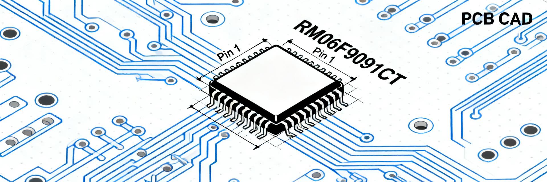
RM06F9091CT Component Report: Specs, Footprint & CAD
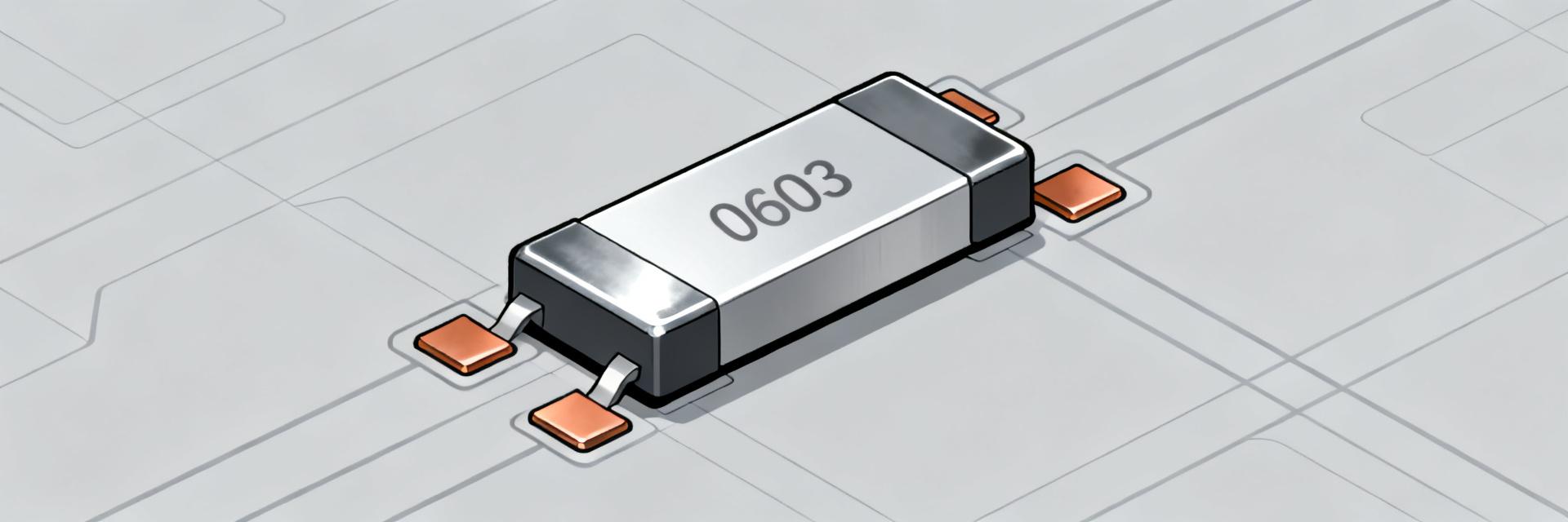
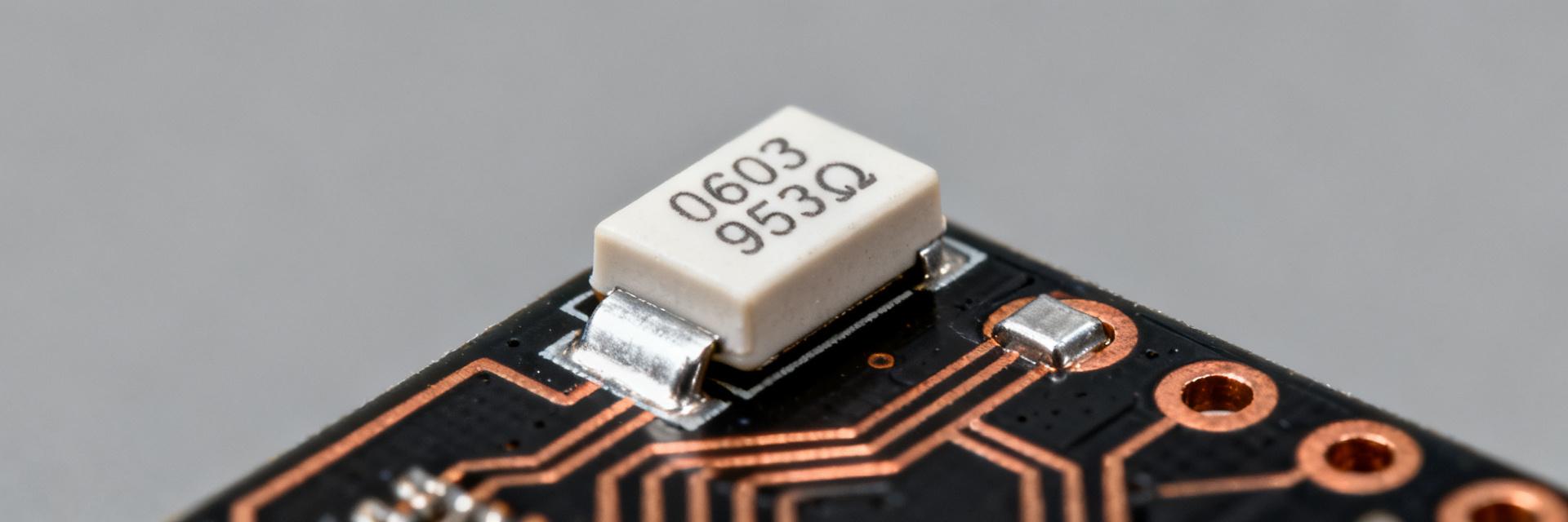
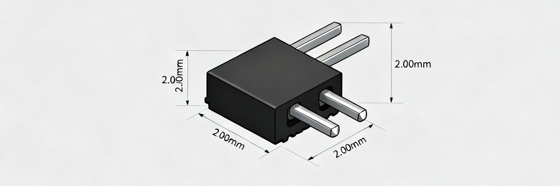
With PCB re-spins and prototype delays frequently traced to incorrect footprints or missing 3D models, verified component data is now a top priority for hardware teams. This report gives you a single-stop technical breakdown of the RM06F9091CT, explaining key specs, recommended PCB footprint guidance, and the CAD formats and verification workflow you should use to avoid costly iterations. Read this before your next prototype run to reduce integration risk and shorten debug time. Background: What RM06F9091CT Is and Where It's Used What the part does Point: The RM06F9091CT is a discrete component intended for use in board-level assemblies where reliable electrical behavior and defined mechanical form factor matter. Evidence: Refer to the part's official datasheet and mechanical drawing for device class, pin count, and package details. Explanation: On a board, this device typically serves as a defined analog/power/digital element (see datasheet for full role), and your selection should link the component's published specs to system-level performance requirements such as voltage range and tolerance. Typical system-level considerations Point: You must plan for thermal, placement, and interface constraints at the system level. Evidence: Datasheet thermal limits, recommended mounting orientation, and recommended clearances are the primary inputs. Explanation: Place the device where its thermal path is clear, avoid heat-sensitive neighbors, allow for test access, and ensure interfaces (signal/power routing) meet impedance and decoupling requirements indicated by the specs table below. RM06F9091CT: Technical Specs & Electrical Characteristics Key electrical parameters to document Point: Capture supply voltages, current ratings, tolerances, thresholds and timing specs into a compact table. Evidence: Pull these values from the official datasheet electrical-characteristics tables and include typical, min/max and test conditions. Explanation: Use the table below to centralize the RM06F9091CT specs for BOM reviewers and validation engineers; this ensures everyone references the same baseline during layout and test. Parameter Typical Min / Max Test Conditions Resistance & Tolerance 9.09 kΩ 9.00kΩ - 9.18kΩ (±1%) 25°C Ambient Power Rating 0.1 W (1/10W) Max 0.1 W Derated above 70°C Operating Temperature - -55°C to +155°C Specified ambient, loaded Max Working Voltage 50 V Max 50 V Continuous DC or AC RMS Test conditions, derating and thermal limits Point: Interpreting test conditions is critical to safe margins. Evidence: Datasheet test conditions specify ambient temperature, measuring points, and mounting assumptions. Explanation: Apply derating rules—reduce max ratings by published margins when ambient or board temperature rises, and add a safety margin (typical engineering practice) for long-term reliability. Document mounting conditions used during test so bench results match field behavior. RM06F9091CT Footprint, Pad Layout & PCB Placement Recommended PCB footprint and pad dimensions Point: Create the land pattern from the mechanical drawing and IPC guidance rather than guessing. Evidence: The manufacturer's mechanical drawing defines terminal geometry and recommended land pattern; map that to an IPC-7351 class for solder fillet and courtyard. Explanation: Extract pad length and width from terminal extents in the mechanical drawing, add solder fillet allowances per IPC class, and set courtyard clearance to at least 0.25 mm greater than the maximum component outline to allow pick-and-place and soldermask registration. Always reference the official drawing for final values. Critical dimensions Use the mechanical drawing origin and units to derive pad center-to-center spacing and pad overlap. Verify pad-to-pad spacing equals the component pin pitch from the drawing; do not rely on reverse-engineered measures from 3D models alone. PAD 1 (GND) PAD 2 (OUT) 0603 Package Pitch: 1.6mm Placement & thermal/assembly notes Point: Placement decisions affect solderability and thermal performance. Evidence: Thermal vias, proximity to large copper pours, and neighboring component heights are common factors called out in assembly guidelines. Explanation: Place the part so heat paths (to internal planes or thermal vias) are consistent with its thermal dissipation rating, leave pick-and-place fiducial space, avoid shadowing by taller adjacent parts during reflow, and reserve testpoints nearby. Use a pre-fab checklist (below) to catch common footprint mistakes such as insufficient soldermask clearance or missing courtyard. CAD Models, Formats & Verification Workflow Common CAD formats and what to download Point: Download authoritative CAD artifacts in formats compatible with your toolchain. Evidence: Recommended formats include STEP (.stp/.step) for 3D, EDA-specific footprint files for your PCB editor (Altium, KiCad, Eagle), and IDF/IPC for board/exchange where supported. Explanation: Prioritize STEP files that include correct origin and units, and ensure your footprint file matches the mechanical drawing—mismatched origins or unit conversions are common causes of assembly errors. Verification steps before use Point: Run a short, repeatable verification sequence each time you import a model. Evidence: Comparative checks between datasheet dimensions and your CAD model catch most issues. Explanation: Follow the checklist below to reduce integration risk and confirm the CAD/footprint pair are assembly-ready. Compare model dimensions to mechanical drawing (origin, units). Import 3D into the board assembly and check Z clearance with enclosure models. Run DRC and DFM checks in your EDA tool (soldermask openings, annular rings). Perform collision checks with adjacent components and fasteners. Validate pick-and-place reference points and BOM MPN mapping. Quick checklist Filename consistency, unit verification, DRC/DFM pass, BOM MPN match, and mechanical drawing attached to the part record. Integration Checklist & Best Practices for Rapid Prototyping Pre-fab validation checklist Point: Provide contract manufacturers a concise packet to avoid misinterpretation. Evidence: Include footprint dims, soldermask openings, courtyard, 3D alignment and thermal via plan in the package. Explanation: Before sending boards, attach the mechanical drawing, STEP model, recommended reflow profile, and a clear BOM row with MPN and alternates. Confirm the CAM engineer has access to IPC class guidance used to generate the land pattern. Post-fab verification and troubleshooting tips Point: Rapid post-population checks speed fault isolation. Evidence: Common failure modes tied to footprint errors include tombstoning, insufficient fillet and solder bridging. Explanation: After assembly, perform a visual solder fillet inspection, basic continuity/power checks, and a targeted functional smoke test; if failures appear, compare pad wetting and fillet geometry against known-good reference boards and adjust land pattern or reflow profile accordingly. Summary Accurate specs, a verified footprint, and validated CAD models shorten development cycles and reduce re-spins. Use the datasheet and mechanical drawing as the single source of truth for RM06F9091CT, apply IPC mapping for land patterns, and follow the verification workflow and checklists above. Use the checklist and verification workflow above before your next prototype run. Frequently Asked Questions How do I verify RM06F9091CT dimensions in CAD? Import the STEP into your CAD, set units to match the mechanical drawing, and measure key features (pin spacing, body outline, terminal extents). Compare those measurements directly to the drawing values and confirm origins. If any mismatch exceeds your assembly tolerance, regenerate the model or correct units before creating the footprint. Which CAD formats should I include with the BOM? Include a STEP file for 3D, the native EDA footprint file (Altium/KiCad/Eagle), and a PDF mechanical drawing. Optionally include IDF or IPC exchange files if your mechanical team requires board-level data. Ensure filenames, units and revisions are clearly tracked in your PLM or parts database. What immediate checks reveal footprint-related assembly failures? Conduct a visual inspection of solder fillets, check for tombstoning or bridging, and verify continuity between expected nets. If issues align with poor wetting or misaligned pads, re-evaluate soldermask openings, pad size and reflow profile before ordering another panel. What are the critical parameters for RM06F9091CT PCB placement? Place the part so heat paths (to internal planes or thermal vias) are consistent with its thermal dissipation rating, leave pick-and-place fiducial space, avoid shadowing by taller adjacent parts during reflow, and reserve testpoints nearby. Always verify pad-to-pad spacing against manufacturer mechanical drawings.