• 73415-1471 MMCX Specs & Sourcing: Compact RF Insights

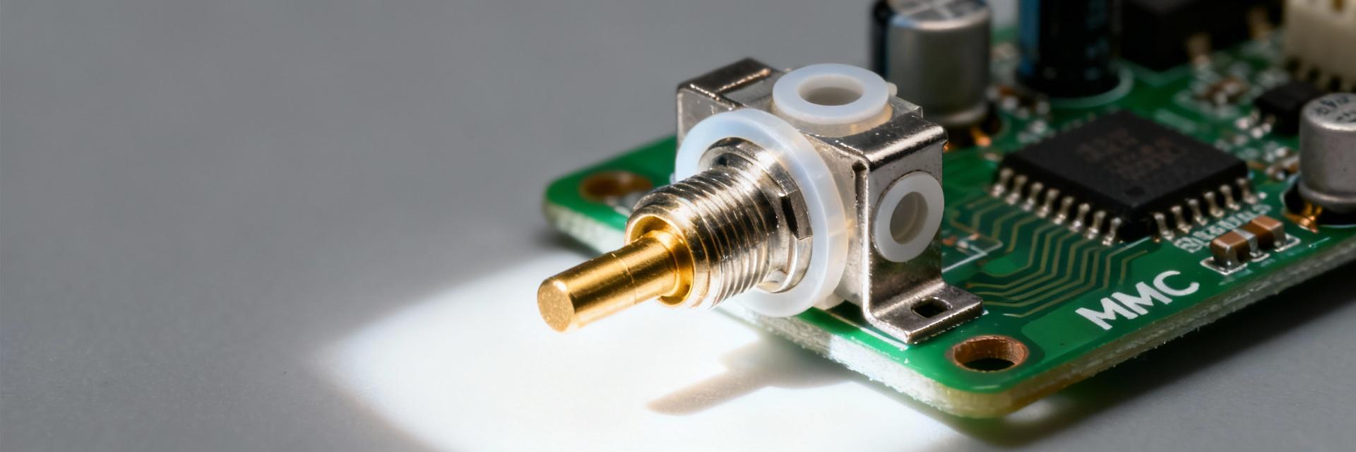
    Compact RF modules demand connectors that balance electrical fidelity with minimal board real estate. This data-driven reference explains the practical implications of 73415-1471 electrical and mechanical specifications. Why 73415-1471 Matters for Compact RF Designs Typical Use Cases & Form-Factor Advantages Point: MMCX PCB jacks are selected for compact radios, RF modules, antenna test points, and handheld devices where space is limited. Evidence: The MMCX form factor offers a low profile and small mating area compared with larger coaxial connectors. Explanation: Designers gain a high-density, space-efficient RF interface that supports test access and removable antennas without a bulky footprint. Electrical vs. Mechanical Trade-offs Point: Choosing MMCX means accepting trade-offs between miniaturization and durability. Evidence: Small center contacts and reduced mechanical bulk yield lower mating durability than larger connectors. Explanation: For high-mating-count applications or severe mechanical stress, consider larger connector families; otherwise, MMCX often provides acceptable retention, rotational freedom, and RF performance for typical portable electronics. 73415-1471 Specifications Deep-Dive Parameter Category Specification Detail Design Impact Impedance 50 Ω (Nominal) Standard RF system matching Frequency Range Up to 6 GHz Suitable for WiFi 6, Bluetooth, Sub-6 LTE VSWR Target < 1.5 across band Ensures signal integrity & power efficiency Materials Brass Body, Gold/Nickel Plating Corrosion resistance & high solderability PCB Interface Through-hole Vertical Jack Supports up to 2.4 mm PCB thickness RF Performance Visualization (VSWR at Frequency) 1G 2.4G 5G 6G *Representative data: Higher height indicates increasing return loss/VSWR within acceptable limits. Performance Testing & Validation 1 RF Test Procedures Key tests include S11 measurements with a calibrated VNA, short launch fixtures to define the reference plane, and time-domain reflectometry (TDR) for transitions. Calibrate the VNA to the connector reference plane to ensure accuracy. 2 Mechanical & Environmental Standard checks include mating/unmating cycle tests, vibration profiles, and thermal soak. Define acceptance criteria (e.g., no loss of retention after 500 cycles) before initiating high-volume procurement. Sourcing, Buying & Cost Considerations Verification & Authenticity ✔ Official datasheet & PN revision check. ✔ Request Certificates of Conformity (CoC). ✔ Batch photos and lot traceability. Pricing & Logistics Cost drivers include plating thickness (Gold over Nickel) and packaging (Tape & Reel vs. Bag). When evaluating cross-references, ensure the footprint and impedance match exactly to avoid costly PCB revisions. Integration: PCB Footprint & Assembly Pro Tip: Layout Optimization Keep a clear RF ground area and use ground vias near the connector barrel. Avoid copper voids under mating contact areas to minimize impedance discontinuities that cause signal reflection. Common Failure Modes Cold solder joints on signal pins Cracked pads from excessive mechanical torque Impedance jumps at the transition point Quick Action Checklist & Alternatives Pre-purchase Checklist Confirm 50 Ω & Frequency Download Datasheet Footprint Order S11/VSWR Samples Request COA / Inspection Selection Criteria If mating cycles exceed 500, consider SMA or high-durability MMCX variants. Use a Prototype → Sample → Qualify → Production workflow to mitigate risk. Frequently Asked Questions How should engineers test 73415-1471 on a PCB for VSWR? + Use a calibrated VNA and define the reference plane at the connector interface. Measure S11 across the intended band, use short launches or fixtures to minimize cable effects, and accept system-specific VSWR targets (typically
  • 47642-0001 Micro USB Type B: Complete Spec Analysis

    This analysis distills mechanical, electrical, mounting, and reliability details engineers need to evaluate integration risk and ensure PCB and assembly compatibility for product designs and sourcing decisions. Connector datasheets and engineering references indicate many legacy and low-cost designs still use Micro USB Type B receptacles; understanding the 47642-0001 nominal dimensions, electrical ratings, and test requirements helps avoid field failures and ensures predictable manufacturability across revisions. 47642-0001: Background & High-level Overview What the part number identifies 47642-0001 denotes a specific Micro USB Type B receptacle family and configuration: a five-contact board-mounted, USB 2.0 class connector intended for standard data and power roles. The part-class implies a mid/surface-mount receptacle with retention features and a shell for mechanical mating alignment, suitable for common board-level connector use cases. Typical applications and why this spec matters Common end products include portable electronics, handheld instruments, accessory modules, chargers, and many legacy IoT devices where compact size and low cost matter. Design drivers focus on footprint, mating cycles, power capability for charging or accessory power, and USB 2.0 data compatibility to ensure interoperability with host devices and cables. Mechanical & Dimensional Specifications Key mechanical dimensions & geometry Key dimensions to verify are overall receptacle footprint, mating depth, shell outer dimensions, pin pitch, and the location of solder tabs or retention posts. Variants typically include right-angle versus straight orientations, mid-mount versus top-mount configurations, and optional through-hole solder tabs for mechanical reinforcement at board edges or internal mounting positions. Materials, plating and mechanical durability Shells are usually stainless or brass-based with conductive plating; contacts are copper alloy with thin gold or nickel finishes to balance contact resistance and solderability. Durability ratings commonly specify insertion/removal cycles; designers should follow handling precautions, ensure mating alignment, and avoid excessive lateral force to prevent contact deformation and premature plating wear. Electrical & Performance Specs (Signal, Power, and EMC) Nominal Voltage 5 VDC Current Rating 0.5–1.0 A USB Protocol 2.0 High Speed Pinout & Signal Integrity The five contacts map to VBUS (power), D+ and D- (USB 2.0 differential pair), ID (accessory/host detect), and GND. For USB 2.0 signaling, maintain controlled differential impedance, minimal stub length on D+/D- traces, and matched pair routing with appropriate termination and common-mode filtering to preserve signal integrity and reduce EMI emissions. Typical nominal ratings are 5 VDC for VBUS and 0.5–1.0 A per contact in many datasheets, with derating recommended for higher temperatures. Contact resistance targets are low milliohm ranges; insulation resistance should be high megohms. ESD withstand and EMI considerations require PCB layout features and, where needed, transient suppression or ground filtering to protect interfaces. PCB Footprint, Mounting & Assembly Guidance Aspect Design Recommendations Land Pattern Design the footprint to capture pad geometry, keepout zones for mating clearance, and drill holes for through-hole tabs if present. Include mechanical reinforcement pads and guard copper pour rules. Soldering Process Follow recommended reflow profiles compatible with contact plating and any lead-free requirements; use wave or hand soldering for large through-hole tabs if specified. Inspection Post-solder inspection should include solder fillet checks and X-ray imaging for hidden joints. Control PCB warpage through symmetric copper distribution. Compliance, Testing & Reliability Case Study Validation Tests Mating/unmating cycle verification (rated cycles). Thermal cycling for solder joint integrity. Vibration and shock for mechanical robustness. Humidity and salt spray for corrosion assessment. Failure Mitigation Frequent failures include bent contacts, plating wear, and board cracking. Mitigation includes: Reinforcing through-hole tabs. Controlling pick-and-place pressure. Pre-production reliability sequences. Selection Checklist & Troubleshooting Guide Actionable Selection Tips Select by mounting type and orientation to match your enclosure. Choose plating to balance contact life and solderability. Confirm current rating and operating temperature range, and verify lead-free process compliance. Include footprint drawings in procurement text such as “47642-0001 footprint” for suppliers. Quick Troubleshooting Start with continuity and contact resistance measurements. Check for bent pins or poor solder fillets. For intermittent faults, clean contacts gently or reflow suspect joints. If board cracking is evident, replace the connector rather than relying on repeated rework. Summary 47642-0001 is a Micro USB Type B receptacle well suited for USB 2.0 devices that need a compact, economical board-mounted interface. Evaluate mechanical mounting robustness, electrical current and voltage ratings, footprint compatibility and targeted reliability testing to ensure production-ready integration and long-term field reliability. ✓ Confirm footprint and mounting variant: ensure pad layout, drill holes for tabs, and mechanical reinforcement align with board edge or mid-board placements. ✓ Verify electrical specs: check VBUS current rating, contact resistance targets, and differential pair routing for USB 2.0 signal integrity. ✓ Plan testing and durability: validate rated insertion cycles, thermal cycling, and solderability; design for easy rework. Frequently Asked Questions What are the critical 47642-0001 footprint checks before PCB release? + Verify pad dimensions, solder mask openings, through-hole placements for reinforcement tabs, keepout for mating clearance, and ensure vias are out of the contact pad areas. Confirm mechanical standoff and board thickness compatibility and validate with a prototype fit test using actual mating cables to catch clearance or interference issues. How do I confirm Micro USB Type B current rating specs are sufficient? + Review datasheet nominal current per VBUS contact and derate for elevated ambient temperatures. If your application draws near or above common 0.5–1 A recommendations, choose a variant with higher rated contacts or implement thermal management. Measure voltage drop under worst-case load to verify acceptable power delivery. When should a connector be replaced instead of reworked on an assembled board? + Replace the connector if contacts are visibly deformed, plating is severely worn, mounting tabs are fractured or the PCB has cracked at the landing area. Rework may be acceptable for isolated solder joint defects, but mechanical damage or repeated intermittent faults usually require replacement to ensure long-term reliability.
  • 501190-2017 Header Deep Dive: Pitch & Footprint Data

    Comprehensive reference for layout, assembly, and procurement decisions for the 501190-2017 dual-row header, focusing on DFM and reliability. Compact PCBs increasingly demand higher I/O density while minimizing board area, pushing engineers toward fine-pitch, dual-row headers. This deep dive gives a practical, dimension-and-footprint-focused reference for layout, assembly, and procurement decisions for the 501190-2017, emphasizing land pattern, soldering, and DFM considerations for reliable production. Quick Technical Snapshot The 501190-2017 is a 20-position, 2-row, vertical SMD header with 1.00mm center-to-center pitch. Constructed with plated contacts over high-temperature polymer, it supports compact board-to-board or cable-to-board interconnects where density and automated assembly are critical. Key Specifications & Procurement Data Specification Typical Value / Engineering Data Positions / Pin Count 20 (2 Rows × 10 Pins) Pitch (Center-to-Center) 1.00 mm (0.0394") Orientation Vertical / Straight Mounting Type Surface Mount (SMD/SMT) Current Rating (Typ.) 0.3–1.0 A per pin Typical Plating Selective Gold or Tin over Nickel Typical Applications Ideal for dense I/O in small enclosures. Common uses include display module mating, FFC/FPC interposers, compact consumer electronics, and embedded sensor interfaces. The 1.00mm pitch balances density with pick-and-place compatibility. Pitch Implications Switching to 1.00mm reduces pad spacing, increasing crosstalk risk and limiting trace clearance. Early layout planning is essential to define microstrip/stripline stackups and maintain signal integrity on 4–6 layer boards. Technical Deep-Dive: Footprint & Soldering Signal Integrity & Power At 1.00mm pitch, impedance control is vital. Maintain trace widths consistent with PCB fab (4–6 mils) and use ground vias for shielding. Route differential pairs on adjacent pins only when required by signal characteristics. Mechanical Reliability Expect smaller solder fillets and higher sensitivity to coplanarity. For boards subject to flex or high insertion forces, consider mechanical anchors or board stiffeners. Define keepouts for rework tools early in the CAD phase. Recommended Land Pattern Geometry Precise land patterns are crucial for wetting and automated placement. Use elongated rectangular SMD pads with rounded ends. Pad Length 1.2 – 1.4 mm Pad Width 0.4 – 0.6 mm Min. Pad Spacing ~0.4 – 0.6 mm Stencil Thickness 0.100 – 0.125 mm Design & Assembly Checklist ✓ CAD Verification: Run pad-to-pad clearance DRC and verify courtyard outlines. ✓ 3D Integration: Fit 3D STEP models into the full-stackup to check interference. ✓ Thermal Profile: Use ramp-soak-peak profile (Peak 235–245°C) for SAC alloys. ✓ Pick-and-Place: Use local fiducials and ensure nozzle sizes are optimized. ✓ Test Strategy: Plan probe/pogo access on the opposite side or via test pads. ✓ AOI Setup: Program AOI to inspect fillet presence, coplanarity, and bridging. Comparative Analysis: 1.00mm Header Density How the 501190-2017 compares in the design ecosystem: Routing Density (Traces/Layer) High Assembly Yield Potential Moderate-High Practical Recommendations for Procurement PROCURE Validate CAD/3D files and assembly behavior prior to volume buys. Request verified land-pattern files, build PCB prototypes with representative solder mask, and run an assembly pilot. Perform mechanical and functional tests to ensure mating connector engagement and electrical continuity before production release. Summary The 501190-2017 combines 1.00mm pitch density with SMD assembly benefits; validate the header footprint early to avoid layout rework. Balance SI and routing by planning stackup and ground stitching; tune stencil apertures and reflow profiles to prevent bridging. Run a CAD/DFM checklist and a pilot assembly to sign off mechanical and electrical acceptance criteria before volume production. Frequently Asked Questions What solder paste and stencil thickness works best? + A 0.100–0.125 mm (4–5 mil) stencil with 60–80% aperture coverage on long pads provides balanced paste volume. Inspect fillets with AOI and modify apertures if bridging or insufficient fillet is observed during the pilot run. Can I use via-in-pad near the header footprint? + Via-in-pad can solve routing congestion but increases cost and risks like entombed solder or plating needs. Prefer staggered vias off the pad edge with microvias. If via-in-pad is necessary, plan for epoxy fill and cap as part of the procurement process. How should I verify the header footprint before production? + Obtain the component STEP/DXF file, import it into your ECAD, and run 3D interference checks. Produce a prototype PCB with representative solder mask, perform an assembly pilot, and inspect solder joints and mating engagement before final sign-off.
  • 1.5mm SMD Header Soldering Guide: SMT Tips & Fail-safes

    Production teams frequently struggle with bridging, poor wetting, placement accuracy, and mechanical reliability when working with 1.5mm SMD header components. This concise, solution-oriented guide focuses on SMT soldering techniques and process controls that improve manufacturability and yield. Why 1.5mm SMD Headers are Challenging Mechanical & Electrical Constraints Small 1.5mm pitch headers have lower pin mass and tighter pin-to-pad geometry than larger connectors, increasing sensitivity to coplanarity and alignment. Thermal imbalance between low-mass PCB copper and relatively higher-mass pins alters local heating, leading to potential cold joints or overheating during reflow. Common Failure Modes Typical defects include solder bridging, tombstoning, insufficient fillets, and misalignment. These defects directly impact yield: bridging (0.5–2%), wetting failures (1–3%), and misalignment (0.5–1.5%). AOI and X-ray are critical for identifying these hidden structural weaknesses. Solderability & Process Data Analysis Thermal Mass & Reflow Profile Range Ramp Rate 1–3 °C/s Soak Time 60–90 s Peak Temp 245–250 °C Target Yield Metrics (Visualized) Metric Target Performance Value Bridging Rate 98% Coplanarity Failures
  • 52745-0897 FFC/FPC Technical Specs & Reliability Data

    Core Engineering Insight Point: Engineers and QA teams need a concise view of the connector parameters that drive design and field reliability. Evidence: Key numbers—0.5 mm pitch, 8 contacts, recommended operating temperature range -40 °C to 85 °C (-40 °F to 185 °F)—are the primary filters during part selection. Explanation: This note consolidates electrical/mechanical specifications and reliability data to help teams decide whether the 52745-0897 is a fit for a given product, and which tests to prioritize for qualification. Qualification Benchmarks Point: Typical qualification benchmarks for 0.5 mm-pitch FFC/FPC connectors illustrate expected minimums. Evidence: Common targets include insertion/extraction cycle endurance of 30–100 cycles for consumer flex use, insulation resistance > 1 GΩ, and stable contact resistance with drift Explanation: “Reliability data” here means lab test results (mechanical, thermal, humidity), contact-resistance drift, and field-return trends summarized for decision-making. Quick-spec snapshot: critical electrical & mechanical parameters Key electrical specs to list and verify Designers should verify electrical ratings and tolerances up front. The following table provides the foundational parameters for verification. Parameter Typical / Spec Visual Indicator Part 52745-0897 ID Verified Pitch 0.5 mm (~0.020 in) Contact count 8 Voltage rating DC 30–50 V ● Stable Current rating 0.5–1.0 A (per contact) ▲ Thermal Check Req. Insulation resistance >1 GΩ (at 500 V DC) Contact plating Gold over nickel ★ High Grade Contact resistance Initial: ~30–60 mΩ typical Nominal Note: Typical versus minimum values should be flagged to avoid surprises. If a specification reads “typical,” require vendor confirmation for worst-case acceptance. Key mechanical & material specs Mechanical form factor and materials dictate assembly and long-term behavior. The connector features: ■ Housing: Thermoplastic with a top-actuated ZIF slider. ■ Footprint: SMD, right-angle or top-contact mating options. ■ Cable Compatibility: Recommended thickness ~0.3–0.5 mm. Design Tip: Include PCB keepout for actuator clearance and reduce solder-paste near the body to limit tombstoning and rework. Reliability testing matrix: lab qualification & expected outcomes Standard test protocols and pass/fail metrics Test Conditions Acceptance Criteria Insertion/extraction cycles 30–100 cycles, room temp ΔR Thermal cycling -40 °C ↔ 85 °C, 10–100 cycles Insulation > 100 MΩ; physical integrity Humidity (85/85) 85 °C/85% RH, 96–240 h No corrosion; ΔR acceptable Vibration / shock Class 3 / specified g levels No contact loss; retention maintained Solderability / reflow Per JEDEC reflow window Good wetting; no void-critical fillets What the numbers mean for system-level reliability Per-connector metrics must be mapped to product usage. If an assembly expects daily cycles, multiply endurance by expected events; for fixed cables, vibration and thermal margins matter more. Apply derating: choose a connector with >2× expected cycles or add mechanical strain relief for higher margin. Measured performance: contact resistance, insulation & environmental data Contact Resistance Stability Initial Rcontact ~30–60 mΩ. Plating, contact force, and contamination drive drift. Use four-wire (Kelvin) measurement to reduce lead errors. Specify ΔR target (e.g., STABILITY RANGE: 60% MARGIN Insulation & Temperature Benchmarks: IR >1 GΩ at room temp. May drop at high humidity/temperature. Chart IR vs temp during qualification to detect moisture ingress or material degradation. ENVIRONMENTAL TOLERANCE: HIGH Design & assembly best practices for long-term reliability PCB Footprint & Soldering Use manufacturer land-patterns and reduce solder paste under the body. Position pick-and-place to avoid actuator contact. Recommended reflow profile follows SnAgCu windows; avoid thermal soak that can deform plastic parts. Cable Handling & Strain Relief Implement clamps or retention posts to remove stress from the FFC termination. Route cables with gentle radii (>5× cable thickness) and provide strain relief that prevents tension transfer to the connector. Failure modes, root-cause signals & mitigation Common failure modes: Intermittent contact (transient ΔR spikes), corrosion (visible discoloration), and solder fatigue (cracked fillets). Triage steps: Visual inspection, continuity under load, thermal imaging for hotspots, and salt-fog exposure for suspected corrosion. Engineering fixes: Improve plating thickness for resistance issues, adjust reflow for solder fatigue, or redesign clip geometry for actuator breakage. Qualification & acceptance checklist for sourcing and production Pre-production Gate Sample lot inspection Full test-matrix execution X-ray of solder joints Formal report with raw data Production Protocols Incoming AQL sampling Dimensional verification Periodic life-sample retesting Traceability label enforcement Summary The consolidated view above gives teams the practical criteria to evaluate the 52745-0897 for a target product. Critical specs—0.5 mm pitch, 8 contacts, initial contact resistance ~30–60 mΩ, and operating range −40 °C to 85 °C—frame the qualification scope. Step 1: Verify Confirm voltage/current ratings and request max contact-resistance values. Step 2: Test Execute insertion/extraction and thermal/humidity cycles based on product use. Step 3: Design Apply land-patterns and strain relief to prevent cable-induced failures. Step 4: Audit Require supplier reports and incoming AQL checks with full traceability. Frequently Asked Questions What tests should be prioritized when qualifying this FFC/FPC connector for consumer products? + Prioritize insertion/extraction cycles that mirror expected user interactions, thermal cycling across the operating range, and humidity (85/85) exposure if the device will see moisture. Use four-wire contact-resistance measurements and inspect solder fillets post-reflow. How should contact resistance be measured to produce reliable comparative data? + Use a four-wire (Kelvin) setup with defined contact force and a stable test fixture. Measure initial Rcontact, then after defined cycle counts and environmental stress. Report absolute values and ΔR against baseline to show drift; include sample size and statistical spread. What immediate mitigations help if field returns show intermittent opens or rising resistance? + Inspect for contamination and corrosion first, check solder joints for fatigue, and confirm cable strain relief. Interim fixes include improved sealing or cleaning; longer-term fixes may require plating changes, adding mechanical supports, or revising assembly profiles and revalidating with the test matrix.
  • 55935-0310 datasheet: Complete spec breakdown & tests

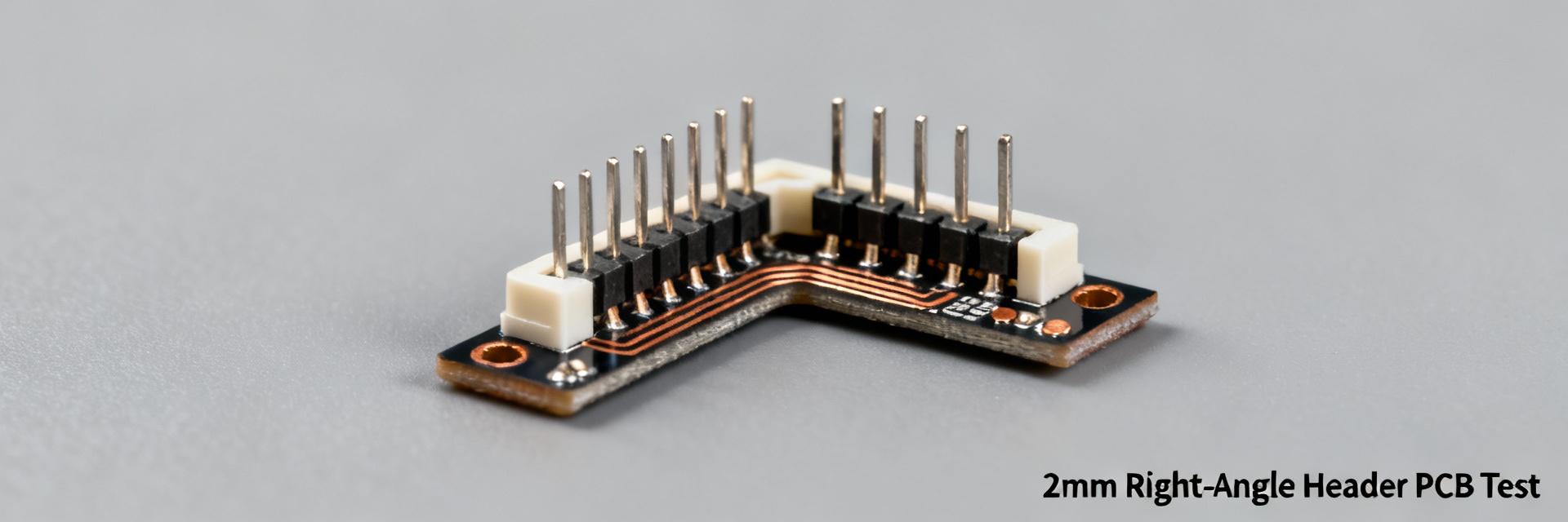
    Point: A systematic datasheet review plus lab validation reduces field failures for wire-to-board headers by making assumptions explicit. Evidence: Key lab metrics include mechanical durability, contact resistance, electrical ratings, solderability, and environmental cycling. Explanation: This article decodes the 55935-0310 datasheet into concise technical specs and reproducible performance tests so engineering teams can verify fit, function, and reliability before PCB commit. Overview: What the 55935-0310 Datasheet Covers Part Summary & Identifiers Confirm core identifiers before ordering. Essential fields: 55935-0310, 2.00 mm pitch, 3 contacts, single row, right-angle through-hole. Always cross-check footprint and variant suffixes to avoid wrong orientation. Typical Applications Commonly used for signal wire-to-board headers, harness interfaces, and low-voltage interconnects. Treat as signal interconnect, not power terminal unless explicitly rated. Mechanical & Physical Technical Specs Dimensions & PCB Footprint ✔ Pitch: 2.00 mm (0.079 in) ✔ Tolerance: 0.1 mm (0.004 in) ✔ Style: Right-angle standoff Materials & Durability Engineered thermoplastic housing and copper alloy contacts. Note boss/locator features for mechanical reinforcement and specify insertion/extraction forces to assess strain relief. Electrical Specifications & Operating Limits Current Derating 60% Margin Recommended safety buffer for elevated temperatures Operating Range -40°C to +105°C Includes self-heating and ambient conditions Contact Resistance < 30 mΩ Initial value per datasheet specification Performance Tests: Lab Validation Guide Test Procedure Condition Measured (Avg) Limit Verdict Contact Resistance (4-wire) Initial/post 500 cycles 15 mΩ / 22 mΩ
  • MPN 42818-0212 Installation: Torque, Pull Tests & Safety

    Installation Criticality Incorrect mechanical installation is a leading cause of connector field failures. Industry audits attribute significant failure rates to mechanical negligence. Incorrect Torque (30%) Inadequate Pull-Testing (25%) Goal & Scope This technical guide establishes a standardized procedure for wire preparation, torque application, and validation for MPN 42818-0212. Following these protocols ensures traceability and reduces variability for bench technicians and field repair teams in the US market. Key Focus: Standardization, Safety, and Quality Documentation. MPN 42818-0212: Overview & Typical Applications Connector Overview & Form Factor The MPN 42818-0212 is a 2-position, 10.00 mm pitch power connector housing designed for board-to-wire and harness applications. It utilizes high-temperature thermoplastic materials with robust metal contact inserts. Prior to installation, technicians must verify pin count, orientation, and vibration class compatibility. Compatibility & Pre-Install Checks Before assembly, cross-reference mating part numbers and approved wire gauges. Always check the insulation OD and retention hardware requirements. Maintain a pre-install checklist and log serial numbers in the assembly record to ensure warranty support and traceability. Torque & Mechanical Specifications Parameter Unit / Requirement Validation Method Target Torque Consult Datasheet (approx. 1 in‑lb ≈ 0.113 N·m) Calibrated Torque Screwdriver Calibration Interval 6–12 Months / 5,000 Cycles QA Calibration Log Pull-Test Force Per Datasheet Minimums (N/lbf) Motorized Pull Tester *Note: Improper torque leads to electrical loss or plastic deformation. Always verify against the specific vendor datasheet before production.* Step-by-Step Installation Procedure STEP 1 Preparation & Crimp Inspection Follow specific strip lengths and use approved tooling. Ensure no frayed strands or excess solder. Visual acceptance includes full conductor capture and insulation support. Document the tooling IDs used. STEP 2 Torque Application Seat terminals fully and mate connectors. Tighten screws in a cross-sequence if applicable. Apply torque in a single controlled motion. Re-check each screw after the full sequence to account for relaxation. Mechanical Pull-Testing Use a calibrated pull tester at a steady rate (25–100 mm/min). Sample 5–10 parts per lot. Record force in N or lbf and identify failure modes. Target force must exceed the thresholds defined in the datasheet. Electrical Validation Confirm integrity via continuity, contact resistance, and insulation resistance (Hipot) tests. Correlate high resistance readings to loose crimps or incorrect torque. Use in-circuit tests for final system verification. Safety & Troubleshooting Safety Precautions • Wear appropriate PPE and follow LOTO procedures. • Observe ESD controls for sensitive circuitry. • Adopt ergonomic practices to prevent repetitive strain. Corrective Actions Symptom: Intermittent contact.Action: Perform pull test → Check torque → Re-crimp with approved tooling if wire is loose. Symptom: Stripped threads.Action: Inspect torque tool calibration → Replace housing and terminal. Key Summary Highlights ✓ Verify datasheet torque and mechanical limits before assembly for traceability. ✓ Use calibrated torque tools (6–12 month intervals) and record values. ✓ Perform pull-tests on 5–10 representative samples per lot and log failure modes. ✓ Run electrical continuity and insulation checks post-installation. ✓ Follow safety-first rework: PPE, LOTO, and ESD controls are mandatory. Frequently Asked Questions What torque should I use for MPN 42818-0212 during installation? You must use the torque value specified in the official datasheet for MPN 42818-0212. If the datasheet is unavailable, pause work to obtain the specification. Example values are estimates only; always verify with the vendor to ensure connection integrity. How many samples should I pull-test for MPN 42818-0212? Typical sampling is 5–10 samples per lot for routine checks. Use a statistically defensible plan based on lot size and risk. Record sample IDs and failure modes; if failures occur, halt production for root-cause analysis. How often should I calibrate torque tools used for this work? Calibrate tools per your QA program, commonly every 6–12 months or after 5,000 cycles. Immediate recalibration is required if a tool is dropped or suspected of damage. Log all calibrations for audit traceability.
  • 51004-0700 Datasheet: 7-pos 2.0mm Housing Quick Specs

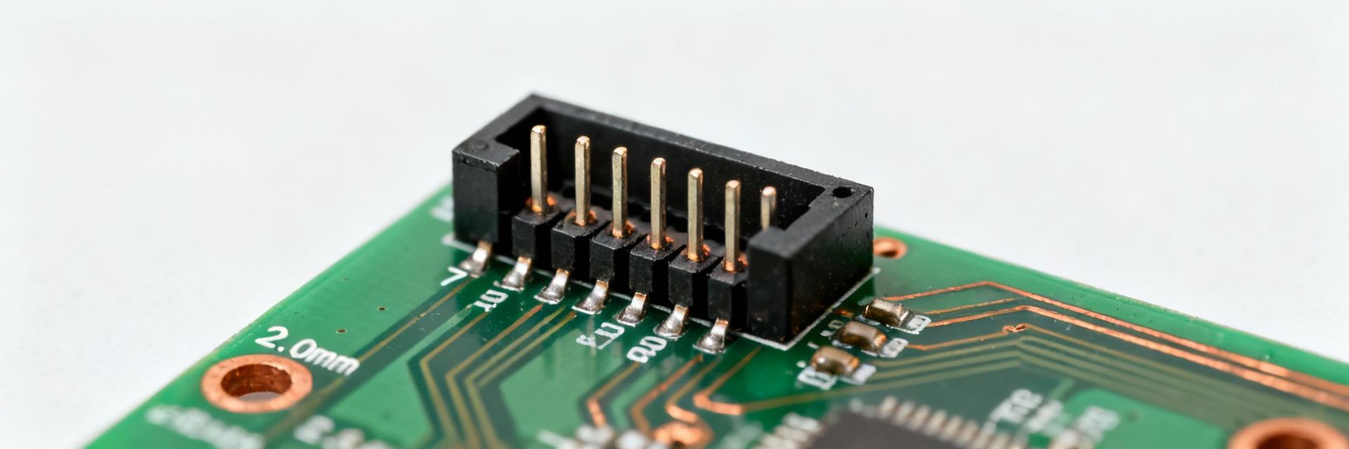
    Professional interconnect solutions for dense signal and light-power applications. The 51004-0700 is a compact, 7-position, 2.0mm pitch wire-to-board/wire-to-wire housing intended for dense signal and light-power interconnects. This quick-specs guide extracts the essential electrical, mechanical, and assembly data so engineers can verify fit, footprint, and procurement notes in one read. The introduction highlights where to check the official datasheet entries for ratings, materials, and dimensional tolerances before CAD or BOM decisions. At-a-Glance Specification Summary Parameter Value / Specification Pitch 2.0 mm Positions 7 Positions Primary Use Compact signal/light-power harnesses Contact Finish Tin or Gold variants (Refer to datasheet) Housing Material Thermoplastic (Refer to flammability class) Mating Cycles Verified per datasheet lifecycle targets Product Snapshot: 51004-0700 Background Key Identifiers & Typical Use Cases Point: The 51004-0700 is identified by its 7 positions and 2.0mm pitch and is commonly referenced on BOMs by its full part number. Evidence: The datasheet entry names pitch and position explicitly for clear procurement. Explanation: On a BOM line list, the full part number, pitch, pos count, and intended function (signal or low-power) should be listed so purchasers and assemblers can match mating housings and verify packing format. Design Integration Point: Designers choose a 2.0mm housing when board density is a priority but moderate current is acceptable. Evidence: The datasheet separates signal-class ratings from power-class ratings, guiding selection. Explanation: Trade-offs are density versus current carrying ability and robustness—use 2.0mm pitch for compact harnesses and signal headers, and reserve larger pitches for higher current or harsher mechanical environments. Quick Specs: Datasheet Technical Summary Electrical & Environmental Highlights The datasheet consolidates rated current, voltage, contact resistance, insulation resistance, and dielectric withstanding voltage under electrical highlights. These fields appear in the technical table that differentiates signal versus power suitability. For signal wiring, prioritize low contact resistance and insulation resistance; for any power use, check rated current and dielectric voltage margins against your worst-case operating and transient conditions. Mechanical & Material Highlights Mechanical and material notes identify housing thermoplastic grade, contact plating options, retention features, and mating cycles. Datasheet material and plating lines define flammability and finishing that affect soldering and longevity. Confirm plating (tin vs gold), latch style, and specified mating cycles—these influence reliability, corrosion resistance, and whether the part meets UL/V-0 or equivalent flammability classifications for your assembly. Pinout, Contact Layout & Wiring Pin Numbering & Orientation Pin numbering and orientation should mirror the drawing in the datasheet and be shown in both schematic and PCB silkscreen. Typical datasheet drawings show a top view with pin 1 marked and sequential numbering across the row. Present a small wiring table mapping pin numbers to functions (e.g., Pin 1 GND, Pin 4 VCC, Pin 7 SIG) so harness builders and firmware teams share an unambiguous reference. Mating & Polarization Physical keys, chamfers, or asymmetrical latches provide polarization and prevent reverse mating. Dimensional drawings describe the recommended mating direction. Mark the PCB silkscreen with the mating direction and pin-1 indicator; call out polarization cues on drawings so automated pick-and-place and manual insertion follow the same orientation rules. Mechanical Dimensions & 3D Assets Critical Dimensions: Extract pitch, overall length/width/height, lead spacing, wall thickness, and latch protrusion as critical dimensions for CAD. The datasheet dimension table lists those values plus recommended tolerances. CAD/3D Guidance: STEP or IGES models should mirror the datasheet outline and include mounting clearances for mating. When creating or importing models, name files with part number and revision, keep mating clearance of at least one pitch height, and place mechanical features on separate layers for easier export to MCAD and ECAD systems. PCB Footprint & Assembly Practices • Footprint Specs: The footprint must match plated-through or SMD pin geometry and allow inspection and rework access. For through-hole variants, use the provided drill sizes and annular ring guidance; for SMD, keep-out areas and solder fillet zones per datasheet. • Soldering Tips: If the housing is reflow-compatible, follow the suggested temperature profile; otherwise, hand-insert and wave-solder or use fixtures to secure housings during soldering to avoid movement or thermal stress. Ordering & Compliance Decoding Part Numbers: Suffixes often indicate color, plating finish, keyed vs. non-keyed options, and packing format. When ordering, verify color, plating (tin/gold), and packaging (tape & reel vs. bag) to match assembly yields and MOQ expectations. Compliance Checklist: Before placing the part on a BOM, run a checklist: electrical ratings, mechanical fit, footprint verification, material flammability (UL/V-0), and required certifications. Request test reports from the supplier if dielectric or mating cycle data is omitted. Summary The 51004-0700 compact 7-position, 2.0mm housing targets dense signal and light-power interconnects. Prioritize verifying electrical ratings, footprint dimensions, and mechanical tolerances against your board and assembly constraints before committing to a BOM. Refer to official datasheet entries for final rated values to ensure fit, reliability, and compliance. Pitch & Power: 2.0mm pitch for signal/light-power use. Footprint: Extract spacing and tolerances carefully. Materials: Confirm thermoplastic class and plating. Assembly: Check mating cycles and packaging. Frequently Asked Questions Q: What electrical specs should I confirm in the 51004-0700 datasheet? Confirm rated current, rated voltage, maximum contact resistance, insulation resistance, dielectric withstanding voltage, and the operating temperature range. These determine suitability for signal or low-power applications and indicate safety margins. Q: How should I prepare the PCB footprint for a 7-pos 2.0mm housing? Use the datasheet’s recommended pad sizes and drill dimensions. Maintain SMD keep-out zones and silk annotations for orientation. Allow inspection clearance and ensure mechanical clearance for the latch and any housing protrusions. Q: What ordering variants and checks prevent procurement issues? Verify variant suffixes for plating, color, and keyed options. Confirm packaging (tape & reel vs. bag) and mating compatibility. Request missing test reports if necessary to validate footprint and assembly before production.
  • 43045-0609 Connector Performance Report: Key Specs

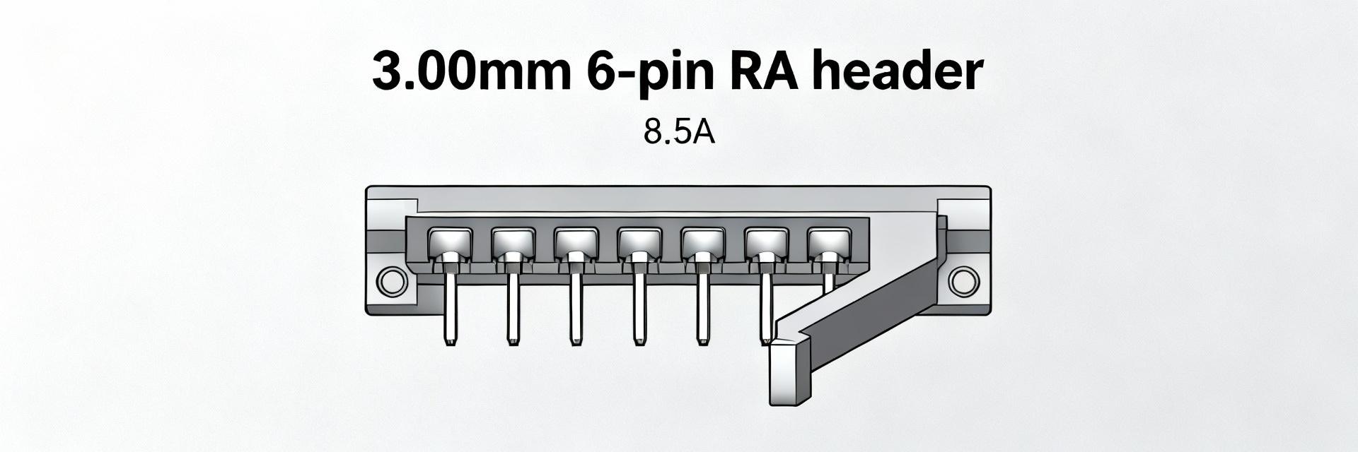
    Across catalog listings and technical sheets, the 43045-0609 presents a consistent electrical envelope and a compact mechanical form. This report unpacks key specifications, practical implications, and provides testing guidance for engineering teams. The 43045-0609 frames relevance for designers assessing power and signal distribution on compact PCBs. Data-driven comparisons pull measured ratings and recommended test conditions into actionable design checks. Current ~8.5 A Voltage 600 V Pitch 3.00 mm Background: what the 43045-0609 is and where it's used Form factor & pinout overview The part is a right-angle, dual-row, 2×3 header with a 3.00 mm pitch and options for solder tabs and board retention. Datasheet callouts show 6 positions arranged 2×3 on 3.00 mm centers and right-angle SMD termination. This footprint targets low-profile board-to-wire power connections where board clearance and mating orientation matter. Simple footprint diagram (labeled dimensions) Feature Dimension Pitch (row) 3.00 mm Rows 2 Positions 6 Mounting Right-angle SMD, optional solder tab Polarization and latch details are typically integrated. Supplier drawings show keyed housings or asymmetrical pinouts and optional latch tangs. Keying reduces mis-mate risk; if your assembly requires board-level retention during reflow or vibration-prone environments, choose the tabbed SMD variant. Typical application environments Typical uses include compact power distribution, control modules, and consumer power subassemblies. The current and voltage envelope and pitch optimize this family for medium-power harnessing on dense PCBs. Expect use where ~5–10 A per contact is needed in a small footprint. Key electrical specifications (data deep-dive) Current, voltage and insulation figures Nominal current ratings are near 8.5 A per contact and voltage ratings approach 600 V, with insulation resistance often ≥ 1,000 MΩ. In practice, derate current for elevated ambient temps or grouped power lanes; parallel contacts can be used for higher total current. Current Carrying Capacity (Max) 8.5 A Dielectric Withstand Voltage 600 V Contact plating, contact resistance & implications Standard finishes are tin; contact resistance ranges vary but are low milliohm order. Tin can oxidize and raise resistance over time—consider gold plating for low-voltage signal integrity or high-cycle applications. Contact finish comparison Finish Typical lifetime (cycles) Best use Tin 100–500 Power-only, low-cycle Gold flash 500–1,000 Mixed signal/power, moderate cycles Gold >1,000 High-cycle, low-voltage signal Mechanical and thermal specifications Mounting & Durability Designers should add anchor pads and avoid large thermal reliefs on solder tabs. Right-angle SMD headers require controlled solder volumes and clearance for mating housings. Follow recommended PCB support areas to resist lever forces. Thermal & Flammability Rated operating temperatures are up to +105 °C with UL 94 V‑0 flammability ratings. Thermal derating is essential—measure thermal rise at intended current and run checks on prototypes to validate design margins. Performance testing & real-world comparison Essential tests include contact resistance, dielectric withstanding voltage, insulation resistance, current-carrying and thermal-rise, solderability, and vibration/shock. Use statistically sound sampling per lot and accelerated aging for production confidence. CHECK Engineering sign-off checklist: ✔ Confirm current per contact and total channel derating ✔ Validate footprint with solder-tab and keep-out zones ✔ Run contact resistance and thermal-rise tests on prototypes ✔ Approve plating finish or specify gold for high-cycle needs Key summary The 43045-0609 is a compact 3.00 mm, 6-position right-angle header delivering ~8.5 A per contact; verify derating for grouped power lanes. Contact finish impacts lifetime—tin is common for power, gold preferred for high-cycle or low-voltage signal applications. Validation must include contact resistance, dielectric withstand, and thermal-rise tests; require clear test conditions on reports. Frequently Asked Questions Is the 43045-0609 suitable for 8–10 A continuous applications? + The nominal rating near 8.5 A per contact can support short-duration or derated continuous applications; confirm thermal rise at intended current and ambient, consider paralleling contacts for higher continuous current, and validate with prototype IR thermal testing. What contact finish should be specified for mixed power and signal use? + For mixed use, gold or gold-flash plating reduces contact resistance growth and supports higher mating cycles for signal pins, while tin can be acceptable for pure power pins. Specify finishes per circuit role. Which lab tests are most critical before volume release? + Prioritize contact resistance after cyclic mating, dielectric withstanding voltage, insulation resistance, thermal-rise under rated current, solderability and vibration/shock. Use IPC/IEC-equivalent procedures. Summary The 43045-0609 combines a compact 3.00 mm, 6-position right-angle package with typical ratings around 8.5 A and 600 V. Validate key electrical and mechanical specs against your loads and follow the selection checklist before procurement to ensure reliable performance.
  • 39012060 connector specs: Complete datasheet & ratings

    Power & Signal 6-Position Dual-Row Introduction In typical power and signal uses, the 39012060 identifier is specified for 6-position, dual-row power harnesses rated for mid-teens amperage per circuit and broad operating temperatures. This introduction summarizes the key datapoints engineers verify on a datasheet—current per circuit, insulation and contact resistance, mechanical retention, and environmental limits—so selection and replacement decisions match field demands. What the 39012060 Connector is: Part Overview & Identifiers Part-Number Anatomy & Common Device Identifiers Point: The numeric code denotes a family-style housing with position and row information. Evidence: Typical catalog entries show a 6-position, 2-row crimp housing with ≈4.2 mm pitch and compatible crimp terminals. Explanation: Read the code as family + position count + configuration to confirm mating geometry and terminal style; when listings include terms like “6-position,” “2-row,” “crimp housing,” they refer to the same canonical attributes for the 39012060 connector. Typical Applications & Where it’s Used Point: This style is chosen where compact multi-pin power is required. Evidence: Common uses include small power supplies, internal wire-to-wire harnesses, appliance control wiring, and industrial control panels. Explanation: The combination of a 6-pin dual-row layout, locking feature, and ~13 A per circuit capability makes the part appropriate for consumer electronics, white goods, and light industrial markets where space and reliable current delivery are both priorities. Datasheet Deep-Dive: Electrical & Mechanical Ratings Electrical Ratings to Verify Point: Key electrical connector specs determine safe application limits. Evidence: Typical datasheet entries list rated current per circuit (≈13 A), rated voltage (application dependent), contact resistance in the milliohm range, insulation resistance in the megaohm range, and recommended wire gauge (commonly AWG 16–22). Explanation: Verify derating curves on the datasheet—elevated temperature or bundling reduces allowable current; look for dielectric withstanding voltage, temperature vs. current derating, and any pulse or inrush ratings to confirm suitability for motor or capacitive loads. Mechanical & Durability Specs Point: Mechanical values impact harness longevity and assembly fit. Evidence: Datasheets typically specify pitch (~4.2 mm), two rows, mating cycles (insert/remove lifecycle), retention/pull-out force, contact type (socket/plug) and termination style (crimp). Explanation: Also confirm housing polymer class, contact plating (e.g., tin or other finishes), and flammability rating (UL 94 class if provided). In panel or harness design, prioritize latch strength and housing stress points where strain relief meets the connector body. Physical Dimensions, Pinout & Mating Specifications Dimensional Drawing Insights Point: Extract a concise set of CAD dimensions for accurate integration. Evidence: Critical dimensions include overall housing footprint, pitch, row spacing, mating height, locking feature extents and cable entry diameter. Explanation: Annotate tolerances on CAD drawings; acceptable ranges typically follow ±0.1–0.2 mm for pitch interfaces and tighter for mating features. Include callouts or an SVG/PDF excerpt that maps each dimension to PCB or harness constraints to prevent interference at assembly. Pinout, Polarity & Mating Point: Correct pin orientation and polarization prevent mis-mating. Evidence: Datasheets show pin numbering, polarization keys, and latch locations; terminals are defined by contact gender and crimp type. Explanation: Confirm mating direction and latch engagement during layout reviews; when replacing parts, match pitch, row count, contact gender and termination style. Use polarization keys or shrouds where available to eliminate reversal risks. Technical Specifications Summary Specification Field Typical Value / Technical Note Visualization Part Identifier 39012060 (6 pos, 2 row crimp housing) Standard Code Positions (Pins) 6 Positions Pitch Spacing ~4.2 mm Current Rating ~13 A per circuit Temp Range −40°C to +105°C Termination Crimp contacts (AWG 16–22) Wire-to-Wire/Board Use-Case Examples & Compatibility Scenarios Case Study A 6-Pin Power Harness for Small Appliances Selection: For continuous 8–10 A load at +60°C ambient, select AWG 18–16 wire. Verify rated ≥13 A per circuit. Insight: If continuous duty pushes temp higher, derate per curves or parallel pins where possible; ensure safety compliance with UL 94. Case Study B Wire-to-Wire Replacement Checklist Strategy: Confirm pitch, row layout, housing orientation, terminal type, and latch geometry. Validation: After replacement, perform continuity and contact resistance checks and a pull test to validate assembly robustness. Installation, Testing & Procurement Best Practices Use the specified crimp die with recommended strip length, inspect crimp height and roll, and perform pull tests along with continuity and insulation resistance checks. Include pass/fail thresholds in procedures—typical resistance limits are low milliohm values; pull forces per terminal family, and insulation resistance >10^6 ohms. Procurement Checklist Buyer items include confirming part ID versus official datasheet PDF, temperature rating, current rating, flammability class, packaging quantity and minimum order. Maintain traceability by recording lot numbers and datasheet revision; contact technical support for lot traceability or custom assemblies. Summary [✓] Confirm electrical limits and derating: verify the rated current, contact resistance and insulation values on the official datasheet to ensure safe continuous operation under your environmental profile. [✓] Validate mechanical fit early: extract footprint, pitch, mating height and latch dimensions to eliminate interference and ensure reliable harness assembly in CAD and prototypes. [✓] Follow inspection and procurement controls: use the crimp/test procedure, record lot traceability, and include final ratings (positions, pitch, current, temp range) in purchase orders and assembly test plans. Common Questions (FAQ) What is the 39012060 connector current rating and how should I derate it? + Typical rated current is about 13 A per circuit on many datasheets, but allowable continuous current drops with higher ambient temperature, bundling or limited ventilation. Use the datasheet derating curve: if operating temperature or harness grouping raises conductor temperature, reduce per-pin current or use larger gauge wire or parallel contacts. How do I perform a 39012060 connector crimp and test procedure? + Use the manufacturer-specified crimp die and recommended strip length, inspect crimp geometry, and run a pull test (per terminal family spec). Perform continuity and contact resistance tests—acceptance often requires milliohm-level resistance—and verify insulation resistance and visual integrity before assembly sign-off. How can I confirm replacement compatibility for a 39012060 connector? + Match pitch, row count, housing orientation, terminal gender and crimp style. Check mating height, latch position and material/temperature ratings on the official datasheet. After physical fit confirmation, perform continuity, contact resistance and pull tests to validate the replacement in the target harness.