
55935-0310 datasheet: Complete spec breakdown & tests
Point: A systematic datasheet review plus lab validation reduces field failures for wire-to-board headers by making assumptions explicit.
Evidence: Key lab metrics include mechanical durability, contact resistance, electrical ratings, solderability, and environmental cycling.
Explanation: This article decodes the 55935-0310 datasheet into concise technical specs and reproducible performance tests so engineering teams can verify fit, function, and reliability before PCB commit.
Overview: What the 55935-0310 Datasheet Covers
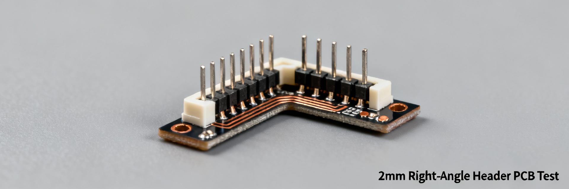
Part Summary & Identifiers
Confirm core identifiers before ordering. Essential fields: 55935-0310, 2.00 mm pitch, 3 contacts, single row, right-angle through-hole. Always cross-check footprint and variant suffixes to avoid wrong orientation.
Typical Applications
Commonly used for signal wire-to-board headers, harness interfaces, and low-voltage interconnects. Treat as signal interconnect, not power terminal unless explicitly rated.
Mechanical & Physical Technical Specs
Dimensions & PCB Footprint
- ✔ Pitch: 2.00 mm (0.079 in)
- ✔ Tolerance: 0.1 mm (0.004 in)
- ✔ Style: Right-angle standoff
Materials & Durability
Engineered thermoplastic housing and copper alloy contacts. Note boss/locator features for mechanical reinforcement and specify insertion/extraction forces to assess strain relief.
Electrical Specifications & Operating Limits
Recommended safety buffer for elevated temperatures
Includes self-heating and ambient conditions
Initial value per datasheet specification
Performance Tests: Lab Validation Guide
| Test Procedure | Condition | Measured (Avg) | Limit | Verdict |
|---|---|---|---|---|
| Contact Resistance (4-wire) | Initial/post 500 cycles | 15 mΩ / 22 mΩ | <30 mΩ | PASS |
| Solderability | Lead-free reflow profile | 95%+ Wetting | Visual coverage | PASS |
+ Recommended Test Procedures & Setups
+ Typical Failure Signatures & Diagnostics
Procurement, PCB Design & Qualification
Pre-purchase
- ☐ Verify pitch, orientation, and contact count.
- ☐ Check lot traceability and packaging options.
- ☐ Order 10–20 evaluation samples for first-run tests.
PCB Layout & Assembly
- ☐ Use silkscreen to mark pin 1 orientation.
- ☐ Provide solder mask keepouts and anchor pads.
- ☐ Ensure through-hole plating thickness meets spec.
"Confirm 2.00 mm pitch, pad diameters and drill sizes per datasheet, silkscreen orientation, solder mask keepout, and mechanical anchor pads."





