
43045-0609 Connector Performance Report: Key Specs
Across catalog listings and technical sheets, the 43045-0609 presents a consistent electrical envelope and a compact mechanical form. This report unpacks key specifications, practical implications, and provides testing guidance for engineering teams.
The 43045-0609 frames relevance for designers assessing power and signal distribution on compact PCBs. Data-driven comparisons pull measured ratings and recommended test conditions into actionable design checks.
Background: what the 43045-0609 is and where it's used
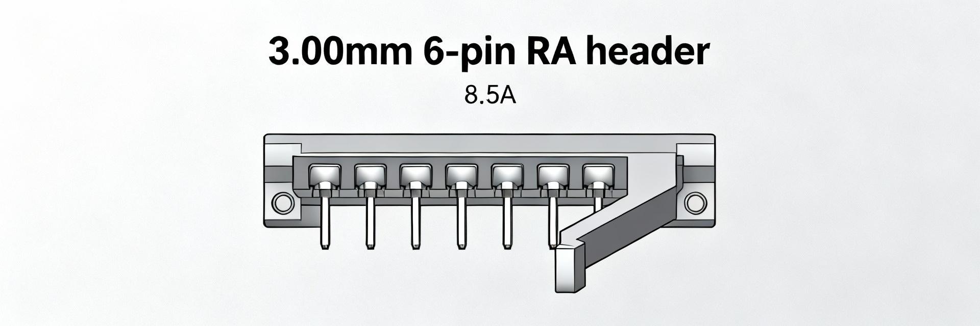
Form factor & pinout overview
The part is a right-angle, dual-row, 2×3 header with a 3.00 mm pitch and options for solder tabs and board retention. Datasheet callouts show 6 positions arranged 2×3 on 3.00 mm centers and right-angle SMD termination. This footprint targets low-profile board-to-wire power connections where board clearance and mating orientation matter.
Polarization and latch details are typically integrated. Supplier drawings show keyed housings or asymmetrical pinouts and optional latch tangs. Keying reduces mis-mate risk; if your assembly requires board-level retention during reflow or vibration-prone environments, choose the tabbed SMD variant.
Typical application environments
Typical uses include compact power distribution, control modules, and consumer power subassemblies. The current and voltage envelope and pitch optimize this family for medium-power harnessing on dense PCBs. Expect use where ~5–10 A per contact is needed in a small footprint.
Key electrical specifications (data deep-dive)
Current, voltage and insulation figures
Nominal current ratings are near 8.5 A per contact and voltage ratings approach 600 V, with insulation resistance often ≥ 1,000 MΩ. In practice, derate current for elevated ambient temps or grouped power lanes; parallel contacts can be used for higher total current.
Contact plating, contact resistance & implications
Standard finishes are tin; contact resistance ranges vary but are low milliohm order. Tin can oxidize and raise resistance over time—consider gold plating for low-voltage signal integrity or high-cycle applications.
Mechanical and thermal specifications
Mounting & Durability
Designers should add anchor pads and avoid large thermal reliefs on solder tabs. Right-angle SMD headers require controlled solder volumes and clearance for mating housings. Follow recommended PCB support areas to resist lever forces.
Thermal & Flammability
Rated operating temperatures are up to +105 °C with UL 94 V‑0 flammability ratings. Thermal derating is essential—measure thermal rise at intended current and run checks on prototypes to validate design margins.
Performance testing & real-world comparison
Essential tests include contact resistance, dielectric withstanding voltage, insulation resistance, current-carrying and thermal-rise, solderability, and vibration/shock. Use statistically sound sampling per lot and accelerated aging for production confidence.
Key summary
- The 43045-0609 is a compact 3.00 mm, 6-position right-angle header delivering ~8.5 A per contact; verify derating for grouped power lanes.
- Contact finish impacts lifetime—tin is common for power, gold preferred for high-cycle or low-voltage signal applications.
- Validation must include contact resistance, dielectric withstand, and thermal-rise tests; require clear test conditions on reports.





