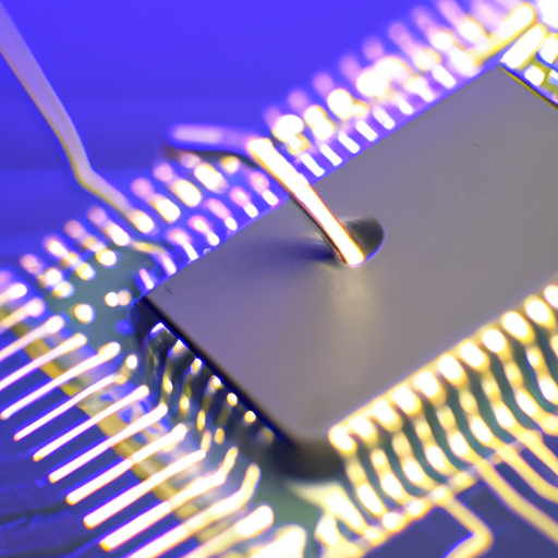
What is the mainstream integrated circuit graduate production process?
What is the Mainstream Integrated Circuit Graduate Production Process?
I. Introduction
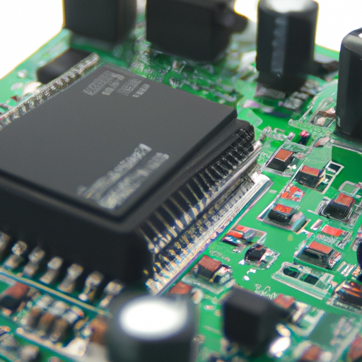
Integrated Circuits (ICs) are the backbone of modern electronics, enabling the functionality of everything from smartphones to supercomputers. These tiny chips, often no larger than a fingernail, contain millions of transistors and other components that work together to perform complex tasks. The importance of ICs in contemporary technology cannot be overstated; they are essential for the operation of virtually all electronic devices. This blog post will provide an overview of the mainstream integrated circuit graduate production process, detailing each stage from design to final testing.
II. Overview of Integrated Circuit Design
A. Conceptualization and Specification
The journey of an integrated circuit begins with conceptualization and specification. This phase involves understanding the requirements of the IC, which may include performance metrics, power consumption, and size constraints. Engineers and designers collaborate to define the specifications that the IC must meet, ensuring that the final product aligns with the intended application.
B. Schematic Design
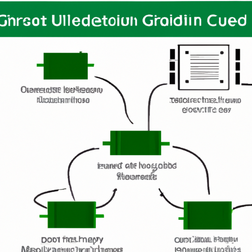
Once the specifications are established, the next step is schematic design. This involves creating circuit diagrams that represent the electrical connections and components of the IC. Designers use specialized software to simulate the circuit, allowing them to validate its functionality before moving on to the next stage. Simulation helps identify potential issues early in the design process, saving time and resources.
C. Layout Design
After the schematic design is validated, the layout design phase begins. This step involves creating a physical representation of the circuit, where the placement of components and the routing of interconnections are meticulously planned. Design Rule Checking (DRC) is performed to ensure that the layout adheres to the manufacturing constraints and standards, preventing errors that could lead to defects in the final product.
III. Fabrication Process
The fabrication process is where the theoretical designs are transformed into physical integrated circuits. This stage is complex and involves several critical steps.
A. Wafer Preparation
The first step in fabrication is wafer preparation. Silicon wafers, which serve as the substrate for ICs, are produced through a process of crystallization and slicing. Once the wafers are created, they undergo cleaning and inspection to remove any contaminants that could affect the quality of the ICs.
B. Photolithography
Photolithography is a key process in IC fabrication. A photoresist material is applied to the wafer, which is then exposed to ultraviolet light through a mask that contains the circuit pattern. The exposed areas of the photoresist are developed, creating a pattern that will guide subsequent etching processes.
C. Etching
Etching is the next step, where the exposed areas of the wafer are removed to create the desired patterns. There are two main types of etching: wet etching, which uses chemical solutions, and dry etching, which employs plasma. This process transfers the circuit pattern onto the silicon wafer, forming the intricate structures that make up the IC.
D. Ion Implantation and Doping
To control the electrical properties of the silicon, ion implantation and doping are performed. This involves introducing impurities into the silicon to create regions with different electrical characteristics, such as n-type and p-type semiconductors. This step is crucial for forming the transistors that will switch and amplify signals within the IC.
E. Deposition Techniques
Deposition techniques are used to add various materials to the wafer. Chemical Vapor Deposition (CVD) and Physical Vapor Deposition (PVD) are two common methods. CVD involves depositing thin films of materials from gaseous precursors, while PVD uses physical processes to deposit materials. These techniques are essential for creating insulating layers and conductive paths within the IC.
F. Metallization
The final step in the fabrication process is metallization, where interconnections between different components of the IC are created. This is typically done using metals such as aluminum or copper, which are deposited onto the wafer to form the necessary electrical connections. The metallization process is critical for ensuring that signals can travel efficiently between different parts of the IC.
IV. Packaging Process
Once the ICs are fabricated, they must be packaged to protect them from environmental factors and to facilitate their integration into electronic devices.
A. Die Preparation
The first step in the packaging process is die preparation. The wafer is diced into individual chips, or dies, which are then bonded to a substrate. This die bonding process ensures that the IC is securely attached and ready for encapsulation.
B. Encapsulation
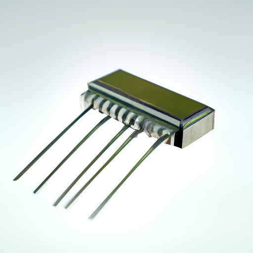
Encapsulation involves enclosing the die in a protective package. There are various types of packaging, including Dual In-line Package (DIP), Quad Flat Package (QFP), and Ball Grid Array (BGA). Each type offers different advantages in terms of size, thermal performance, and ease of assembly. Proper encapsulation is essential for providing thermal and mechanical protection to the IC.
C. Testing and Quality Assurance
Before the packaged ICs can be shipped, they undergo rigorous testing and quality assurance. Functional testing checks whether the IC operates according to its specifications, while reliability testing assesses its performance under various conditions. This step is crucial for ensuring that only high-quality products reach the market.
V. Final Testing and Quality Control
The final testing and quality control phase is critical for ensuring the reliability and performance of the integrated circuits.
A. Electrical Testing
Electrical testing involves two main types: parametric testing and functional testing. Parametric testing measures the electrical characteristics of the IC, such as voltage and current levels, while functional testing verifies that the IC performs its intended functions correctly.
B. Reliability Testing
Reliability testing is conducted to assess the long-term performance of the IC. Burn-in testing subjects the IC to elevated temperatures and voltages to identify early failures, while environmental testing evaluates the IC's performance under extreme conditions, such as temperature fluctuations and humidity.
C. Yield Analysis
Yield analysis is an essential part of the production process, focusing on understanding yield rates and identifying strategies for yield improvement. High yield rates are crucial for the economic viability of IC manufacturing, and continuous monitoring and optimization of the production process are necessary to achieve this goal.
VI. Conclusion
In summary, the integrated circuit production process is a complex and multi-faceted journey that transforms conceptual designs into functional electronic components. From the initial design stages to the final testing and quality control, each step is critical for ensuring the performance and reliability of the ICs. As technology continues to evolve, the industry is witnessing trends such as miniaturization, increased integration, and the adoption of advanced materials, all of which will shape the future of IC manufacturing. Continuous innovation in this field is essential for meeting the growing demands of modern technology and ensuring that integrated circuits remain at the forefront of electronic advancements.
VII. References
1. Academic journals and articles on semiconductor manufacturing.
2. Industry reports and white papers from leading semiconductor companies.
3. Books on integrated circuit design and fabrication processes.
This blog post provides a comprehensive overview of the mainstream integrated circuit graduate production process, highlighting the critical stages involved in bringing these essential components to life.

