


Helping you save cost and time.

Provide reliable packaging for your goods.

Quick and reliable delivery to save time.

Excellent after-sales service.
New Product Launch
More +

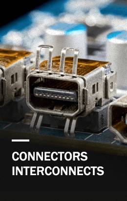
Hot Selling Parts


Blog
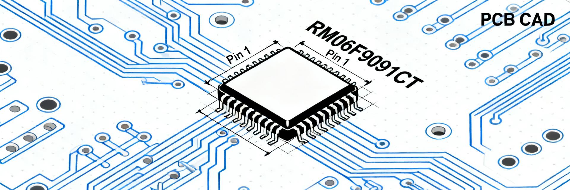
RM06F9091CT Component Report: Specs, Footprint & CAD
With PCB re-spins and prototype delays frequently traced to incorrect footprints or missing 3D models, verified component data is now a top priority for hardware teams. This report gives you a single-…
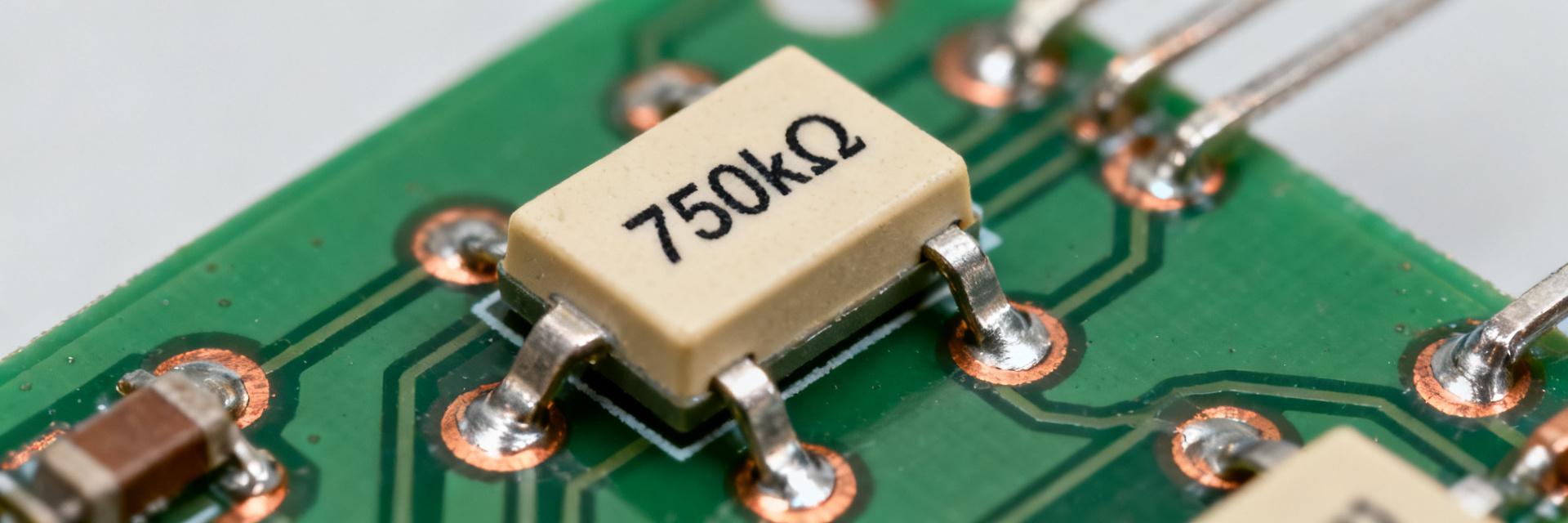
0603 SMD Resistor 750kΩ 1% — Detailed Specs & Datasheet
Point: 0603 components dominate high-density PCB assemblies, and designers often need high-value, tight-tolerance resistors for analog filtering and precise biasing. Evidence: many modern consumer and…
RM06F73R2CT SMD Resistor: Measured Specs & Thermal Data
2026-05-27 10:15:22
RM06F9530CT Datasheet: 0603 953Ω 1% Specs & Test Data
2026-05-25 21:49:07
47745-0100 Complete Specs: Pinout, Current, Dimensions
2026-05-23 16:32:09
353630260 Connector Specs Report: Pin, Pitch & Ratings
2026-05-23 16:15:09
26-01-3114 Specs Deep Dive: Pitch, Mount & Pinout Explained
2026-05-23 15:34:07
Read more