527461071 Datasheet Breakdown: Key Specs & PCB Tips
Key Takeaways (GEO Summary)
- Space Efficiency: 0.5mm pitch reduces connector footprint by ~40% vs 1.0mm alternatives.
- Durability Insight: 20-cycle rating optimizes costs for "set-and-forget" internal modules.
- Critical Layout: Bottom-contact design requires strict FPC orientation for signal integrity.
- Yield Optimization: 60-80% stencil aperture prevents bridging in high-density 0.5mm layouts.
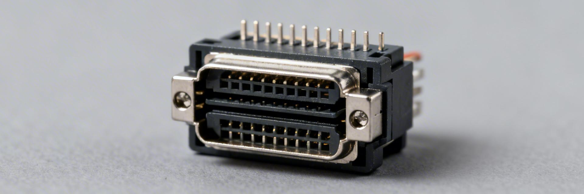
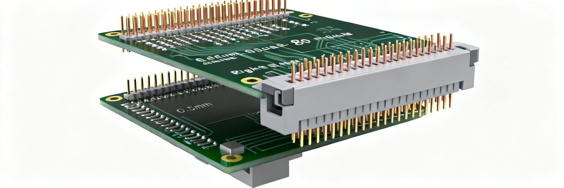
The 527461071 datasheet calls out a compact 0.5 mm‑pitch, 10‑position right‑angle SMT FFC/FPC connector with bottom contacts and a short rated durability (approximately 20 mating cycles). This overview distills the datasheet into the electrical, mechanical and soldering parameters engineers must verify, and provides concrete PCB tips to avoid assembly failures and field issues. Use this breakdown as a rapid cross‑check before layout and production.
| Feature | 527461071 Specs | Standard Industrial Equiv. | User Benefit |
|---|---|---|---|
| Pitch Size | 0.5 mm | 1.0 mm | Saves 50% PCB area |
| Contact Type | Bottom Contact | Top/Dual Contact | Lower profile height |
| Mating Cycles | 20 Cycles | 50+ Cycles | Reduced BOM cost for internal cables |
This article follows a checklist approach: identify the tables and drawings to read first, confirm electrical derating and contact finish, validate recommended land pattern and reflow curve, then apply PCB tips for pad geometry, mask openings and keep‑outs to reduce tombstoning, bridging and contact damage.
Quick part overview & datasheet at-a-glance
What the part identifier and form factor tell you
- Part code maps: 0.5 mm pitch → 10 positions → right‑angle orientation → bottom contacts; verify exact suffixes for contact finish and tape/reel options.
- Form factor implies low profile and board‑edge seating; check mechanical drawing for board edge clearance and seating depth.
- Key specs tables: mechanical drawings, electrical ratings, and recommended land pattern are highest priority.
- Connector family tables will list plating, insulating material and mating direction—capture these for PCB and process specs.
- Durability table (mating cycles) and environmental limits are critical for lifecycle assessment and warranty claims.
How to read the datasheet efficiently
Start with the front mechanical drawing and recommended footprint, then scan electrical ratings and environmental limits. Locate contact finish and plating notes, mating procedure diagrams, and the reflow profile or solderability statement. This order surfaces show‑stoppers early and focuses verification on manufacturability and service life.
- Confirm pitch, position count and orientation against the board CAD model.
- Capture contact plating, current/voltage ratings, and mating cycles.
- Save the recommended land pattern and reflow notes into the PCB spec sheet.
Expert Review: Senior Hardware Engineer
By Marcus V. | PCB Layout Specialist
"When integrating the 527461071, the most common failure isn't electrical—it's mechanical stress. Because of the 20-cycle limit, I recommend adding a silkscreen bracket on the PCB to indicate the 'Locked' vs 'Unlocked' position of the actuator. Also, ensure your FPC stiffener is exactly 0.3mm thick (check the drawing!) to prevent contact intermittency."
Key electrical specs to confirm
Contact arrangement, pitch and current/voltage ratings
Verify the contact count and 0.5 mm pitch, and confirm the connector is specified for low‑power signal use rather than power delivery. The datasheet lists maximum rated current and voltage per contact; apply a safety margin (typically 50% derating for continuous operation) when signals share connectors with higher ambient temperatures or reduced cooling.
Contact resistance, insulation resistance and temperature range
Contact resistance figures indicate expected insertion loss and should be compared to system sensitivity. Typical milliohm‑level resistance is acceptable for signals but becomes critical for low‑voltage, high‑speed nets where contact impedance affects integrity.
Mechanical specs & reliability parameters
Mating cycles, retention force and mechanical tolerances
A rated durability of roughly 20 cycles implies the connector is intended for limited mating events — factory assembly is the primary use case. Interpret mating cycles relative to expected field operations: devices with frequent user cable insertion require higher durability or mechanical strain relief.
PCB design & layout tips (actionable PCB tips)
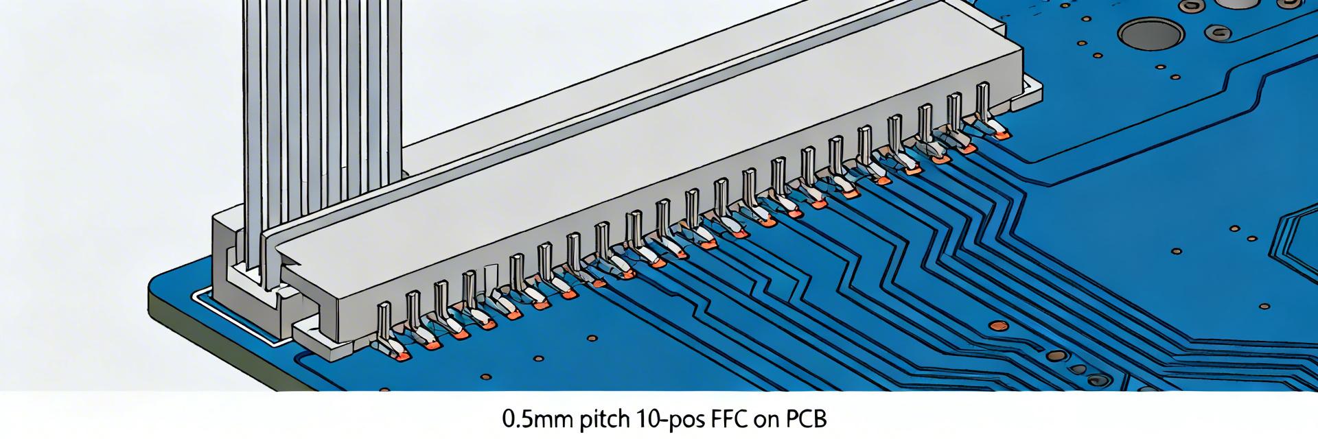
Recommended footprint, solder mask and stencil guidance
Follow the recommended footprint precisely: pad lengths and spacing at 0.5 mm pitch leave little tolerance for deviation. Use 60–80% paste aperture for small pads to balance wetting and prevent paste collapse.
- Pad dimensions: Match datasheet; prefer rounded ends for paste release.
- Solder mask: Defined openings between pads to control bridging.
- Stencil: 60–80% pad coverage; consider thieving for long pad banks.
Assembly, testing & common pitfalls
Typical assembly failures and prevention
Common failures include solder bridging, insufficient fillet, misalignment and bent contacts. Root causes are typically incorrect paste apertures, inaccurate pick‑and‑place nozzle programming, or reflow profiles that exceed component limits.
Summary
Verify the connector’s pitch and position, electrical ratings and mechanical tolerances, and follow the recommended reflow and footprint guidance before committing to layout. Capture solder mask and stencil rules, and run pilot assemblies to validate the PCB tips and process windows.
FAQ
The datasheet rates the connector for limited mating cycles (approx. 20), indicating it is intended for factory assembly rather than frequent field mating.
Common mistakes include oversized paste apertures and missing mask between pads, leading to bridging and tombstoning at the 0.5mm pitch.
Avoid via-in-pad unless plated and capped. Vias beneath pads can wick solder away, weakening the mechanical joint of the SMT lead.