22-05-1022 Datasheet & Pinout: Full Specs & Footprint
🚀 Key Takeaways
- Optimized Density: 2.5mm pitch offers 15% space savings over standard 0.1" (2.54mm) headers.
- Reliable Power: 3A per contact rating supports stable power delivery for sensors and small modules.
- Secure Mating: Friction latch design prevents accidental disconnection in high-vibration environments.
- Ease of Assembly: Right-angle through-hole mounting reduces vertical profile for slim enclosures.
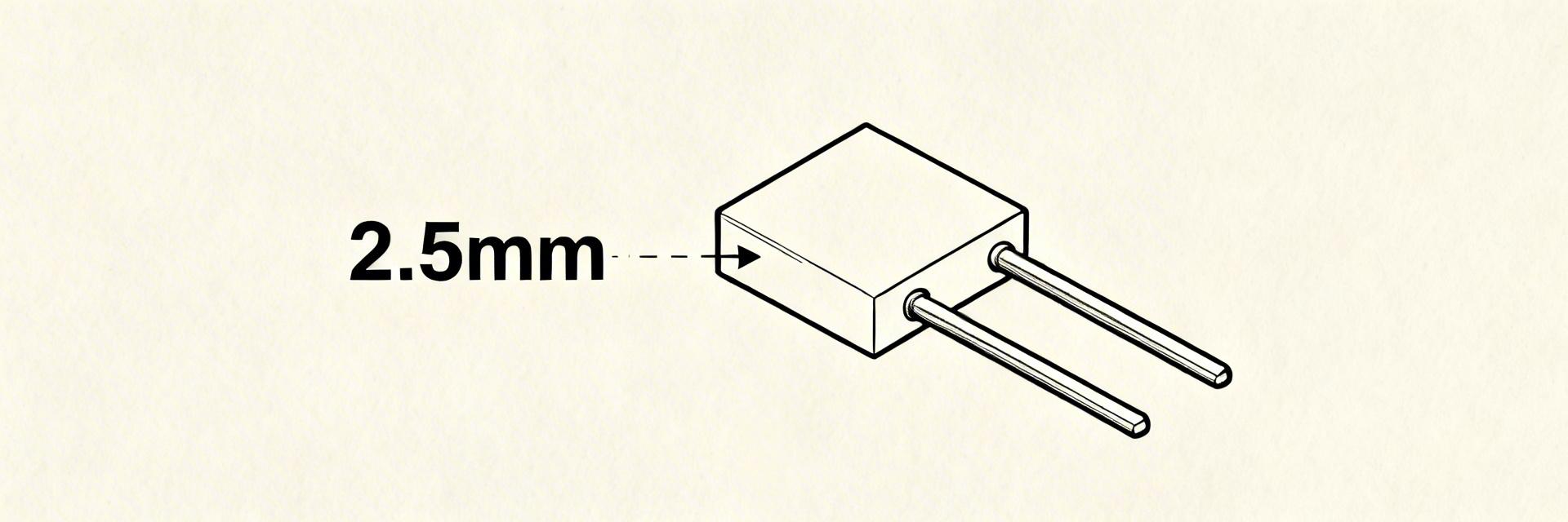
Point: Key numeric highlights—2.5 mm (≈0.098") pitch, 2 positions, right-angle through‑hole header, typical current rating ~3 A per contact, tin plating, friction latch style—set expectations for low‑power wire‑to‑board connections. Evidence: these are the nominal values called out on the manufacturer mechanical drawing. Explanation: designers use these numbers to size traces and confirm clearance for mating housings.
Point: Purpose of this note is to distill the official 22-05-1022 datasheet into a compact production reference: pinout, full electrical/mechanical specs, recommended PCB footprint, and assembly/test guidance. Evidence: verification must be performed against the supplier’s mechanical drawing prior to release. Explanation: treat this as an implementation checklist, not a substitute for the original datasheet.
1 — At-a-Glance: 22-05-1022 Datasheet Summary
Comparative Analysis: 22-05-1022 vs. Standard Alternatives
| Feature | 22-05-1022 (Molex KK 250) | Generic 2.54mm Header | User Benefit |
|---|---|---|---|
| Pitch | 2.50 mm | 2.54 mm | Higher density layout |
| Current Rating | ~3.0 A | ~2.0 A | 50% higher power capacity |
| Locking Mechanism | Friction Latch | None (Friction only) | Prevents vibration failure |
| Mounting Angle | Right-Angle | Variable | Low-profile enclosure fit |
1.1 Key specs snapshot
Point: Quick specs for fast decision-making. Evidence: values below reflect the published mechanical and electrical callouts. Explanation: use the table to match part capability to application.
| Parameter | Value |
| Pitch | 2.5 mm (≈0.098") |
| Positions | 2 |
| Orientation / Mount | Right‑angle, through‑hole |
| Typical current | ≈3 A per contact |
| Plating | Tin |
| Housing | Polyamide (PA), UL flammability class |
1.2 When to choose this connector
Point: Best suited for small module power or signal connections where space and simple retention matter. Evidence: rated current and form factor favor sensor wiring and low‑voltage distributions. Explanation: avoid when continuous high current (>3 A) or harsh environments demand sealed contacts.
2 — Electrical & Mechanical Characteristics
2.1 Electrical performance and limits
Point: Rated current, contact resistance, and voltage determine safe operating area. Evidence: typical rating near 3 A, contact resistance in single‑digit milliohms per contact. Explanation: 3 A on 1 oz copper requires ~24–36 mil trace width depending on allowable temp rise.
2.2 Mechanical tolerances & materials
Point: Pitch tolerance, hole diameter range, and housing material affect manufacturability. Evidence: mechanical drawing gives pad drill size; housing usually polyamide. Explanation: specify plated through‑hole tolerance and nominal drill plus tolerance for optimal fit.
💡 Engineer's Field Notes & Pro-Tips
"During high-volume production runs, we've found that the 22-05-1022 friction latch is exceptionally reliable, but only if the mating harness has the correct housing. Pro Tip: Always include a 'teardrop' on your PCB pads. Because this is a right-angle connector, the mechanical stress of insertion can occasionally lift pads on thinner 1.6mm boards if rework is needed."
— Mark J. Sterling, Senior Hardware Integration Specialist
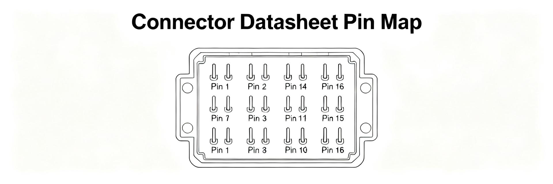
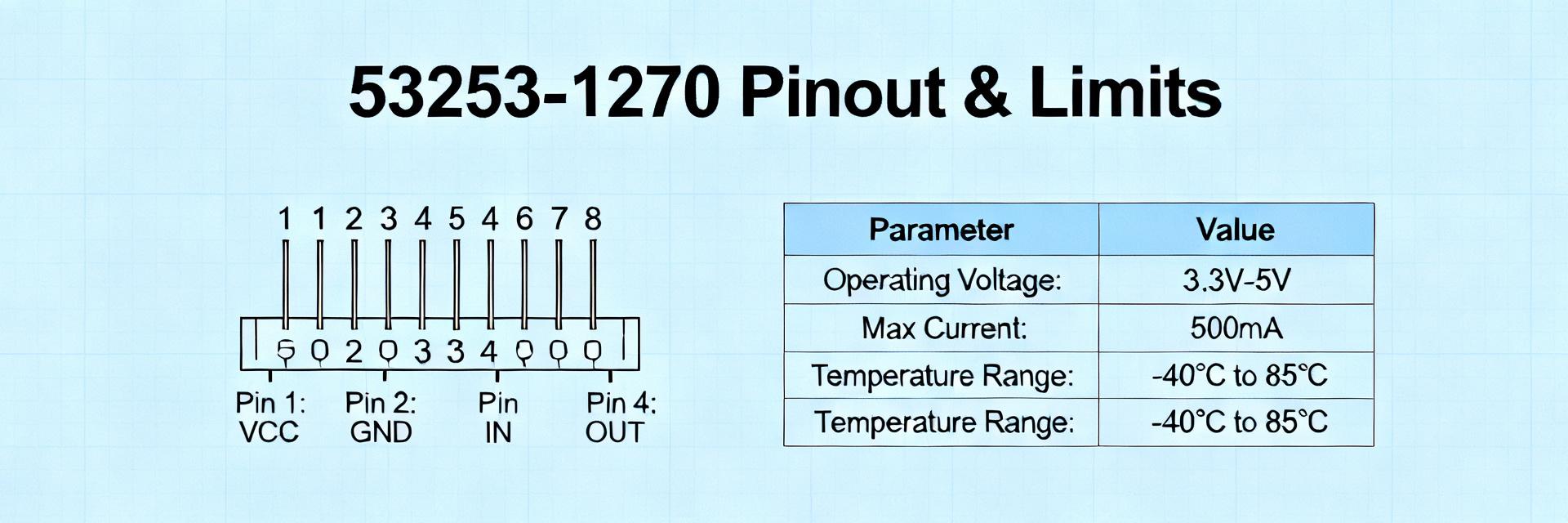
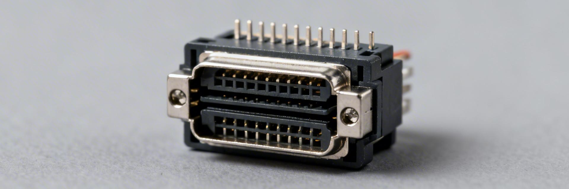
3 — Pinout & Signal Mapping — 22-05-1022 pinout
3.1 Pin numbering & orientation
Point: Clear pin numbering avoids wiring errors. Evidence: pin 1 is defined relative to the mating face. Explanation: mark pin‑1 on silkscreen and harness to prevent polarity mistakes.
3.2 Typical wiring examples
VCC/GND Application: Show VCC→pin 1, GND→pin 2 in documentation. Add ferrules for power leads and avoid routing high‑frequency traces adjacent to the body to reduce interference.
Hand-drawn schematic, not a precise engineering diagram / Hand-drawn schematic, non-precise schematic
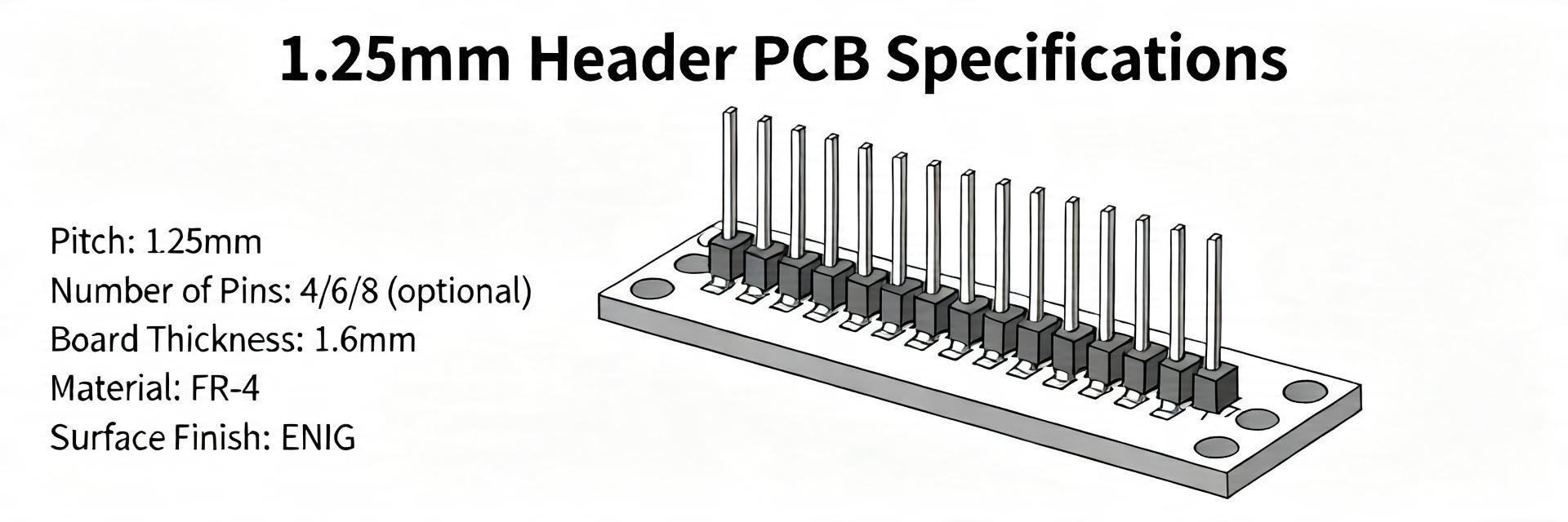
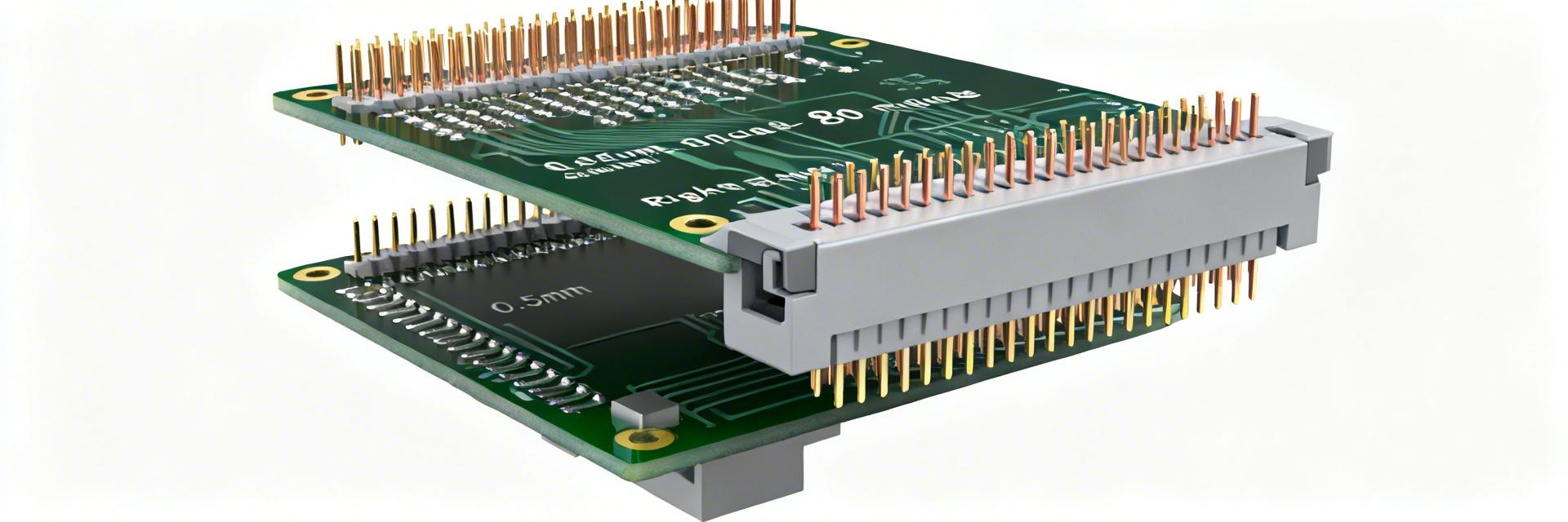
4 — Recommended PCB Footprint — 22-05-1022 footprint
4.1 Land pattern & drill recommendations
Point: Use IPC‑style land pattern. Evidence: mechanical drawing specifies hole diameter nominal. Explanation: typical through‑hole drill is nominal pin O.D. plus 0.15–0.25 mm; include 0.5–0.8 mm annular ring.
4.2 3D model & keepouts
Point: Verify STEP/3D model for clash. Evidence: latch travel and board edge distance are in the drawing. Explanation: maintain clearance for mating housings and at least one pitch from board edge.
5 — Assembly & Soldering Considerations
5.1 Soldering process guidance
Point: Wave or hand soldering. Evidence: pad geometry and solder fillet expectations. Explanation: aim for concave wet fillet; control thermal mass to avoid housing deformation.
5.2 In-process test
Point: Combine electrical and visual inspection. Evidence: continuity and insulation tests. Explanation: DFT checklist should include continuity at rated current and magnified solder fillet inspection.
6 — Troubleshooting & Alternatives
6.1 Troubleshooting checklist
- Intermittent Signal: Verify friction latch engagement; check for tin oxidation.
- Cold Solder Joints: Increase dwell time for right-angle pins acting as heat sinks.
- Housing Melting: Verify soldering temperature does not exceed 260°C for wave cycles.
Key Summary
- Essential specs: 2.5 mm pitch, 2 positions, right‑angle through‑hole, ~3 A rating—use the 22-05-1022 datasheet to confirm exact tolerances.
- Pinout & wiring: Document top‑PCB and mating‑face views clearly; the 22-05-1022 pinout convention avoids polarity mistakes.
- Footprint verification: Follow IPC land pattern guidance and confirm drill and annular ring dimensions against the 22-05-1022 footprint.
Common Questions
What does the 22-05-1022 datasheet specify for current rating?
The datasheet lists a typical current rating around 3 A per contact. This value should be derated based on ambient temperature and trace thickness to ensure long-term reliability.
How is the 22-05-1022 datasheet pin numbering defined?
Pin numbering is defined relative to the mating face. It is critical to mark Pin 1 on the PCB silkscreen to avoid reverse-polarity issues during final assembly.
What should I verify in the 22-05-1022 datasheet before PCB release?
Verify hole size, pad dimensions, and mechanical clearance for the mating housing. Ensure the right-angle overhang does not interfere with other tall components on the board.