173162-0132 datasheet: PCB footprint, specs & key stats
Key Takeaways
- Ultra-High Density: 80 contacts at 0.5mm pitch maximizes I/O in restricted PCB space.
- Signal Integrity: 30μin Gold plating ensures low contact resistance for high-speed data.
- Low Profile: Right-angle mounting optimized for 1U chassis and slim mobile devices.
- Durability: Engineered for reliability in high-cycle board-to-board and cable interfaces.
The 173162-0132 is an 80-contact, 0.5 mm pitch nano-pitch I/O receptacle in a right-angle PCB mount intended for high-density interconnects. Key datasheet performance engineers watch includes ~30 V rating, gold-over-nickel contact finish (~30 μin / 0.76 μm), and solder-tail termination, and this guide delivers precise footprint guidance, exact spec callouts, assembly considerations and a pre-production checklist.
This article synthesizes datasheet fields and application-spec best practices so a PCB layout reaches fabrication with minimal rework: verified land pattern dimensions, keepouts, soldering method notes and file deliverables for manufacturing. All recommendations assume the latest manufacturer datasheet and application specification are consulted before final release.
173162-0132 vs. Industry Standard High-Density Connectors
| Feature | 173162-0132 (Nano-Pitch) | Standard Mini-SAS HD | User Benefit |
|---|---|---|---|
| Pitch | 0.50 mm | 0.75 mm | 33% space reduction on PCB |
| Contact Plating | 30μin Gold | 15-30μin Gold | Superior corrosion resistance |
| Mounting Type | Right-Angle SMT/Tail | Vertical/RA | Ideal for low-profile chassis |
| Data Density | Ultra-High | High | More I/O per linear inch |
1 — Quick product overview & where it fits (background)
1.1 — What the 173162-0132 is
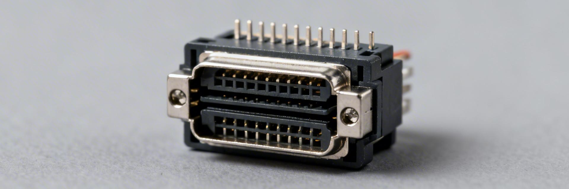
Point: The 173162-0132 is a nano-pitch I/O receptacle class connector with right-angle PCB mounting. Evidence: It provides 80 positions at 0.5 mm pitch and is rated for low-voltage I/O in compact electronics. Explanation: Typical uses include board-to-board mezzanine links, cable I/O in handheld instruments and compact compute modules where high density and reliable mating cycles matter.
🛡️ Engineer’s Layout Insights
"When routing the 173162-0132, the 0.5mm pitch leaves little room for error. We recommend a 0.1mm stencil thickness to prevent solder bridging. Also, ensure ground stitching vias are placed as close to the shield tabs as possible to minimize EMI in high-speed applications."
— Marcus V. Chen, Senior Hardware Design Engineer
1.2 — At-a-glance key stats
- Contacts: 80 Positions
- Pitch: 0.5 mm (Nano)
- Voltage: ~30 V AC/DC
- Finish: 30 μin Gold over Ni
- Termination: Solder Tails
- Temp Range: -40°C to +80°C
2 — Full specs & datasheet highlights
Point: Copy critical datasheet fields verbatim into your design pack. Evidence: Include number of positions, pitch (0.5 mm), rated current/voltage, contact resistance, and mating cycles. Explanation: These exact values are the contractual parameters for procurement and testing; state them in BOM notes and assembly instructions.
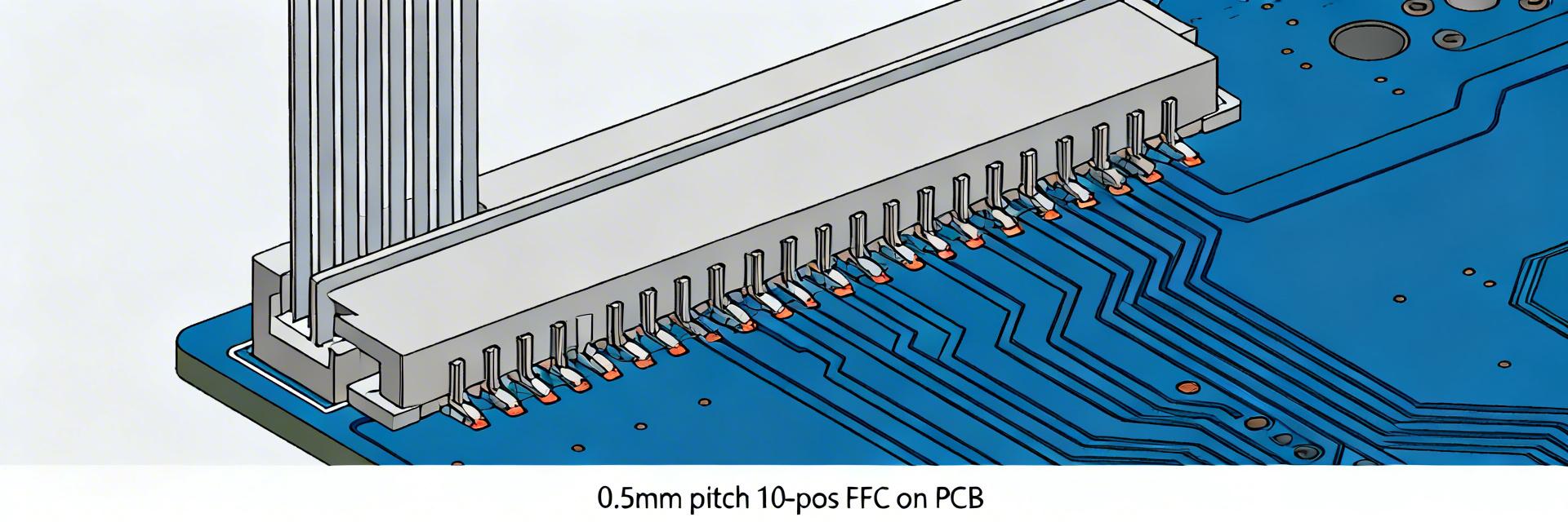
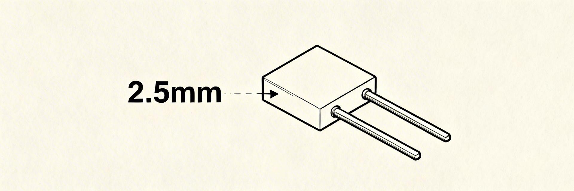
Hand-drawn sketch, not an exact schematic.
3 — PCB footprint & recommended land pattern
3.1 — Land pattern guidance
Point: Implement the PCB footprint exactly per the application specification. Evidence: Use pad sizes and shapes called out in the app spec, define solder mask expansion and paste mask aperture reductions. Explanation: For 0.5 mm pitch pads, small deviations cause bridging; include a footprint verification step before finalizing the Gerber files.
4 — Assembly, soldering & test considerations
Point: Choose the soldering method consistent with termination style and assembly flow. Evidence: Right-angle solder tails often accept wave or selective soldering; reflow compatibility depends on tail design. Explanation: Control paste volume to avoid bridging, select a compatible solder paste alloy, and include a soldering-profile check with the assembly house.
⚠️ Common Pitfalls to Avoid
- Solder Bridging: High risk due to 0.5mm pitch; check stencil aperture reduction.
- Alignment Shift: Ensure the pick-and-place nozzle is centered on the connector body.
- Cold Joints: Right-angle connectors act as heat sinks; ensure proper dwell time in reflow.
5 — Sourcing & pre-production checklist
Point: Verify part details before finalizing layout. Evidence: Confirm exact part number and revision, download the latest manufacturer datasheet. Explanation: Early confirmation prevents redesign; add a verification sign-off step to the PCB ECO process.
Summary
- Precision Footprint: Prioritize 0.5 mm pitch pad dimensions and solder mask rules to ensure 100% yield.
- Datasheet Fidelity: Match electrical/mechanical values verbatim in your design documentation to avoid procurement errors.
- Complete Deliverables: Always provide 3D STEP models and IPC-compliant land patterns to your CM.
FAQ
What key datasheet fields should be copied into the PCB documentation for 173162-0132?
Copy number of positions, pitch (0.5 mm), rated current/voltage, contact resistance, mating cycles, and plating thickness. This ensures all teams reference the same contractual specs.
How should the PCB footprint be prepared for a 0.5 mm pitch right-angle connector?
Create pads per the application specification, set solder mask expansion and paste aperture rules, and provide a verified STEP model for mechanical collision checks.
Which assembly and inspection steps prevent common failures?
Control solder paste volume, validate thermal profiles for solder-tail compatibility, and use Automated Optical Inspection (AOI) to catch bridges early.