52465-1071 Connector: 0.031in Pitch & Height Report
Key Takeaways (GEO Summary)
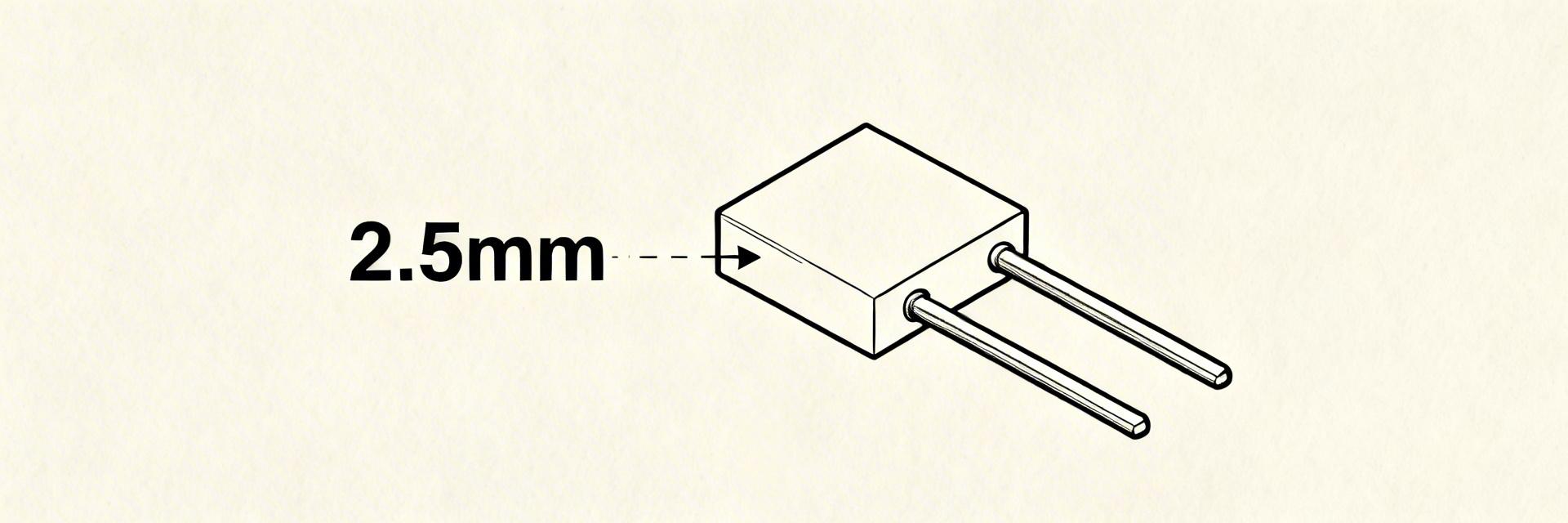
- Space Efficiency: 0.8mm (0.031in) pitch reduces lateral board footprint by ~30% vs. 1.27mm standards.
- Design Flexibility: Mated heights from 4.5mm to 7.0mm allow precision vertical stack optimization.
- Signal Integrity: SMT termination supports high-speed data paths but requires TDR validation.
- Production Yield: High-density SMT layout necessitates AOI and precision stencil control for 99%+ yield.
Miniaturization in board-to-board interconnects is driving widespread adoption of sub-1.0 mm pitches for compact consumer and industrial systems. This brief analyzes the 52465-1071 connector family with a focus on its 0.031in / 0.8 mm pitch and multiple mated-height options, assessing mechanical design implications, signal integrity trade-offs, manufacturability, and procurement actions to move from prototype to production.
Benefit: Increases I/O density by 40% in the same linear space, enabling smaller wearable and IoT device PCBs.
Benefit: Eliminates thru-holes, freeing up the bottom PCB layer for additional component routing or shielding.
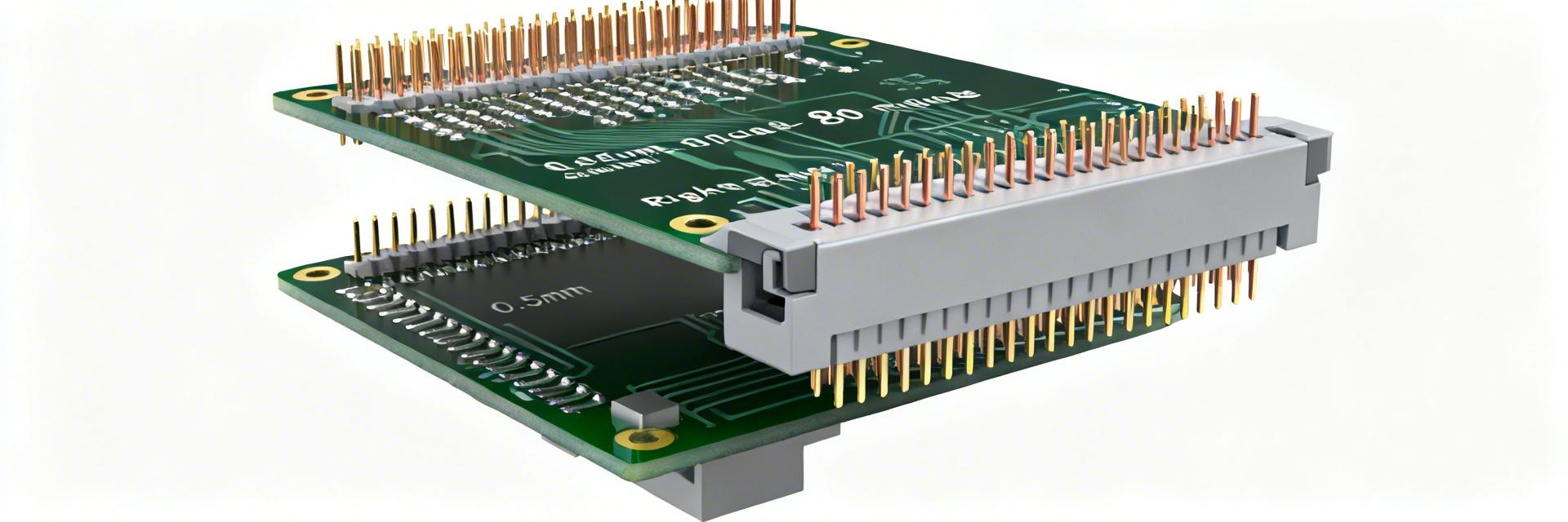
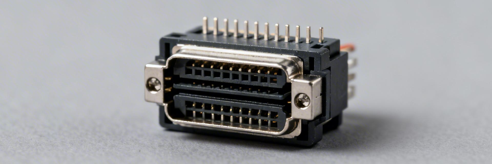
Connector background — 52465-1071 at a glance
Basic specification snapshot
Point: The connector is a single-row, surface-mount board-to-board interface optimized for thin-stack assemblies. Evidence: Typical offerings specify a 0.031in / 0.8 mm pitch, single-row layouts with contact counts matching the row length, and SMT termination. Explanation: These attributes make it suitable for mezzanine stacks where board area is limited but precise placement and solder quality are required; designers should verify exact rated voltage/current and plating options with the datasheet before selection.
| Attribute | 52465-1071 Series (0.8mm) | Generic 1.27mm Header | User Advantage |
|---|---|---|---|
| Pitch | 0.031in (0.8 mm) | 0.050in (1.27 mm) | 36% Space Saving |
| Mated Height | 4.5–7.0 mm | Fixed (~6.0mm) | Modular Stack Control |
| Mounting Type | SMT (Surface Mount) | THT or SMT | Automated Pick-and-Place |
| Signal Density | High (12.5 pins/cm) | Low (7.8 pins/cm) | Better for Multi-signal I/O |
Typical application contexts & constraints
Point: Use cases include thin-stack modules, handheld consumer electronics, and compact industrial modules where vertical density matters. Evidence: The small pitch reduces lateral board area and enables tighter board stacks. Explanation: While 0.031in pitch supports space-limited designs, it is less suitable for high-current paths or harsh-field connectors; designers must assess thermal dissipation, clearance for enclosures, and isolation for mixed-power designs when selecting a specific mated height and plating.
Pitch implications — 0.031in pitch: electrical & mechanical trade-offs
Signal integrity & electrical limits
Point: Tight pitch increases crosstalk risk and constrains trace routing for controlled impedance. Evidence: At 0.031in pitch, adjacent contact spacing reduces available conductor separation, affecting differential pair spacing and return-path design. Explanation: Use microstrip or stripline routing with careful return-path continuity, increase pair spacing where possible, and validate with TDR and eye-diagram tests; limit per-pin current per datasheet and distribute power across multiple pins when needed.
Principal Interconnect Architect
"When working with 0.8mm pitch like the 52465-1071, common failure points are 'solder wicking' into the contact area. I always recommend a 0.1mm stencil thickness with a 1:1 aperture ratio. If your stack-up allows, keep your high-speed differential pairs on the layer immediately below the top ground plane to minimize the loop area at the connector transition."
Mechanical tolerances & assembly yield
Point: Small pitch raises placement and soldering sensitivity, increasing bridging and insufficient fillet risks. Evidence: Typical assembly tolerances tighten to ±0.05 mm or better and require precise paste volume control. Explanation: Specify tighter PCB fabrication tolerances, use stencil-controlled paste deposition, and include AOI and selective X-ray inspection checkpoints to detect bridging and voiding early in the process; document acceptance criteria in the PCB assembly plan.
Height variants — comparative metrics
| Metric | Lower Height (~4.5 mm) | Higher Height (~7.0 mm) |
|---|---|---|
| Stack thickness | Minimized (Ultra-thin devices) | Increased (Modular systems) |
| Mechanical stability | Lower | Higher |
| Engagement tolerance | Smaller | More forgiving |
| Vibration resistance | Requires reinforcement | Better native resistance |
Typical Application: Wearable Tech Stack
Using the 4.5mm height variant in a smartwatch PCB assembly to minimize Z-height while maintaining 10 redundant ground pins for EMI shielding.
Design checklist — integrating a 0.031in pitch connector
PCB layout & footprint best practices
Point: Footprint precision and solder-mask strategy directly influence yield at 0.031in pitch. Evidence: Narrow land patterns require controlled solder mask expansion and exact annular rings to avoid bridging. Explanation: Use manufacturer-recommended land patterns where available; if not, follow IPC guidelines with reduced pad size, 0.15 mm minimum annular ring where possible, solder mask-defined pads, and place vias outside the immediate pad ladder or use capped vias; include keep-out zones for adjacent components and clearance for mate alignment features.
Assembly & thermal process considerations
Point: Reflow profile and paste deposition critically impact wetting and tombstoning risk. Evidence: Small pads with uneven paste volumes cause insufficient wetting or tombstoning during reflow. Explanation: Validate a controlled reflow profile with appropriate soak and peak temperature for lead-free processes, optimize stencil aperture ratios for consistent paste volume, and reserve hand-solder only for repairs; include post-reflow AOI, X-ray for hidden joints, and a defined repair workflow in assembly documentation.
Summary (conclusion & next steps)
Core findings: The 0.031in pitch connector family supports significantly denser board stacks and flexible mated heights, but demands tighter PCB fabrication tolerances, disciplined paste deposition, and a focused SI/ME validation plan.
- Verify pitch and footprint dimensions against the datasheet and 3D models before PCB release; ensure 0.031in pitch clearance and pad geometry are confirmed.
- Order evaluation samples across the available heights and perform mating-cycle and contact-resistance tracking to evaluate lifecycle effects on reliability and signal margins.
- Integrate TDR/eye-diagram testing and mechanical shock/vibration profiles into the validation plan to quantify SI and mechanical robustness.
FAQ — common questions
Smaller pitch reduces space for pair spacing and return-path continuity, increasing crosstalk risk; mitigate with internal stripline routing, increased pair spacing where feasible, and validate with TDR and eye-diagram testing to confirm acceptable margins.
Choose a mid-to-higher mated height to improve mechanical leverage and engagement tolerance, and add alignment bosses or reinforcement to reduce contact stress; verify with vibration and shock testing to establish pass/fail criteria.
Request datasheet confirmation of pitch (0.031in / 0.8 mm), available mated heights, plating and solderability details, 3D STEP files, and sample kits for each height variant; include inspection criteria for first-article review.