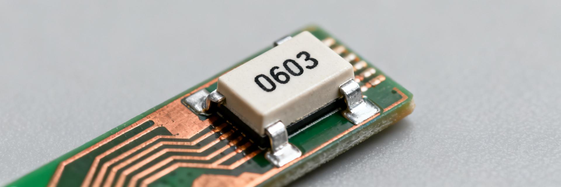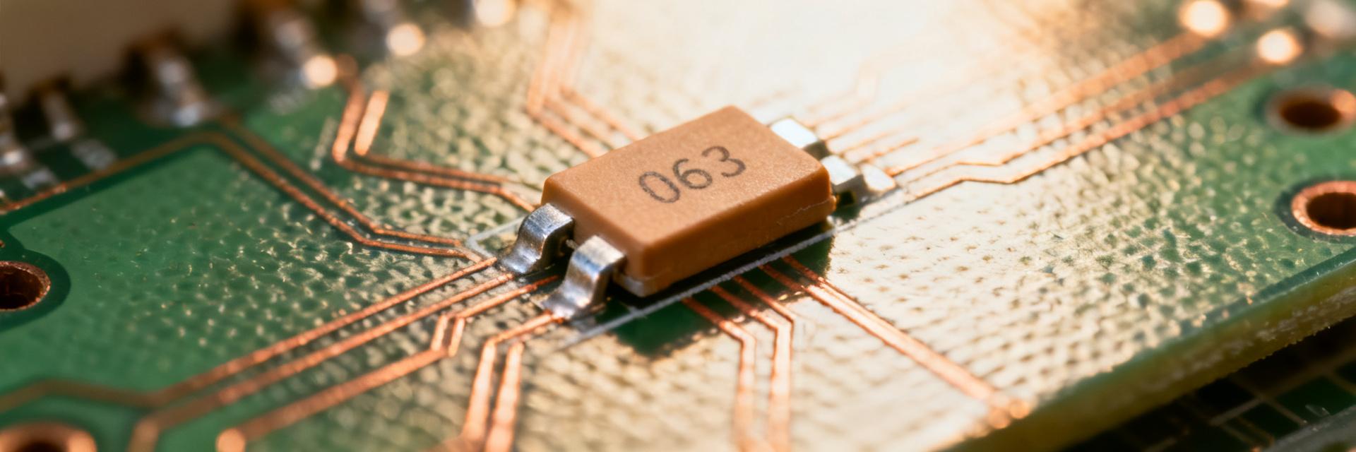
53647-0274: Especificaciones Eléctricas Completas y Hoja Rápida
The 53647-0274 connector datasheet consolidates mechanical and electrical limits you must check before layout. This dual-row, 0.635 mm pitch mezzanine header offers 20 contacts, nominal 500 mA per contact and ~100 V dielectric rating. Use this page as a single-page technical reference to confirm pinout, footprint and stack-height choices.
Designers reviewing BOMs will verify contact finish, mating cycles and board clearance early to avoid rework. The following sections translate key specs into actionable layout and test checks so you can select the right stack height, plating and solder pattern for reliable prototypes and production runs.
Connector overview & intended applications

Form factor & pitch
Point: The part is a 0.635 mm pitch, dual-row, 20-contact vertical mezzanine header intended for board-to-board stacking.
Evidence: Small pitch and vertical SMT pins favor tight-profile stacked modules.
Explanation: You will choose this form factor when you need compact interconnects for daughtercard modules, mezzanine radios, or sensor stacks where minimal X–Y footprint and low profile are priorities.
Variants & stacking options
Point: Two common mated stack heights are offered to suit different board separations.
Evidence: Typical available mated heights are about 8.0 mm and 14.0 mm, selectable by variant.
Explanation: Select the lower height for compact enclosures and the taller for assemblies needing room for connectors, shielding or component clearance between boards; variants often share a single part family.
53647-0274 connector datasheet — Electrical ratings & key specs
Current, voltage & resistance ratings
Point: Electrical specs drive whether pins are used for power or signals.
Evidence: Rated current per contact is 500 mA, dielectric rating ~100 V, and typical maximum contact resistance near 70 mΩ with insulation resistance in the GΩ range.
Explanation: You should reserve these pins for low-power rails or signals; parallel contacts or a dedicated power connector are better for higher currents.
Contact finish, plating thickness & reliability metrics
Point: Finish affects mating reliability and corrosion resistance.
Evidence: Gold contact finish near 0.25 µm improves low contact resistance and reduces fretting corrosion; expected mating cycles vary by spec sheet.
Explanation: For frequent mating cycles choose the thicker gold finish; for few-cycle, lower-cost finishes may suffice but verify contact resistance after environmental stress tests.
Mechanical & stacking specifications
Height above board & mechanical envelope
Point: Mechanical envelope determines clearance and component placement.
Evidence: Height-above-board and mated/unmated stack heights define the vertical tolerance budget.
Explanation: During layout reserve keep-out zones above and below the header, account for tolerance stack-ups, and confirm the chosen stack height permits any shielding or adjacent tall components without mechanical interference.
Solder retention & mounting
Point: Robust solder joints prevent failures in stacked assemblies.
Evidence: Solder-tail geometry and optional guide pins influence retention during reflow.
Explanation: Use recommended land patterns, consider additional vias for mechanical anchoring, and avoid routing high-stress traces near pads; if available, include board guides or stiffeners for assembly rigidity.
53647-0274 connector datasheet — Pinout, numbering & PCB footprint
Pin numbering diagram & signal assignments
Point: A consistent pin numbering convention prevents wiring errors. Evidence: Pins are typically numbered 1–20 across two rows (A/B or odd/even mapping), with common patterns assigning edges to GND or VCC. Explanation: Map signals so high-frequency pairs are adjacent where needed, reserve multiple pins for ground returns, and document odd/even mapping clearly in your schematic and assembly drawings.
Recommended PCB land pattern & footprint details
Point: Land pattern geometry influences solder fillet and yield. Evidence: Pad length and width, solder mask dams, and thermal reliefs are specified for reliable SMT joints. Explanation: Follow the recommended pad dimensions, include small mask slivers between pads on 0.635 mm pitch to reduce solder bridging, and place micro-vias or annular rings per the manufacturer’s footprint guidance.
Materials, environmental ratings & test data
Insulator & contact materials
Verify Tg of the insulator for your reflow profile and confirm contact base material for acceptable conductivity and mechanical spring properties under repeated mating.
Environmental limits & qualification
Evaluate operating temperature range, run thermal cycle and vibration tests, and consider salt spray if the assembly sees corrosive environments.
Practical design checklist & prototyping tips
Design checklist before PCB layout
Verify every checklist item against the component drawing and your enclosure constraints, then freeze the footprint before panelization to avoid expensive mask changes.
Assembly, testing & validation tips
Use a prototype rig to exercise mating durability, perform contact-resistance spot checks after assembly, and select bed-of-nails or flying-probe tests appropriate for your test plan.
Technical Specification Summary
| Parameter | Typical Value |
|---|---|
| Pitch | 0.635 mm |
| Contacts | 20 (dual-row) |
| Rated current | 500 mA/contact |
| Dielectric rating | ~100 V |
| Contact finish | Gold ~0.25 µm |
Key summary
- Confirm pitch and layout: 0.635 mm dual-row, 20 contacts—ensure your land pattern, mask splits and solder fillets reduce bridging and yield problems.
- Electrical checks: Rated 500 mA per contact and ~100 V dielectric—use multiple pins or a power connector for higher currents and reserve ground pins for returns and EMI control.
- Mechanical selection: Choose 8.0 mm or 14.0 mm mated heights per board separation needs; include board guides or stiffeners for stacked assemblies to avoid stress on solder joints.
Common questions and answers
What should you verify in the 53647-0274 connector datasheet before layout?
Check pitch, pin numbering convention, stack height variants, contact plating thickness, current and voltage ratings, and recommended land pattern. Validate thermal limits and mechanical envelope against your enclosure, and confirm mating cycles and finish to match expected field use and assembly methods.
How do you interpret the pinout for signal vs. power assignments?
Identify ground and power distribution patterns, reserve multiple parallel pins for higher currents, and keep high-speed differential pairs paired and close to reference returns. Map odd/even or row A/B numbering in schematics and ensure documentation for assembly and test fixtures is unambiguous.
What prototyping tests should you run for this mezzanine header?
Perform continuity and contact-resistance checks, mating-cycle durability tests, and a reflow compatibility check. Use a mechanical stress test for board stacking, run thermal cycling representative of the product environment, and validate EMI behavior with your chosen ground routing strategy.