43045-1012 Hoja de datos Análisis profundo: Especificaciones eléctricas clave
The official datasheet consolidates the limits every engineer must respect; this article opens with a single data hook: the part’s published continuous current and dielectric test values govern trace sizing, clearance, and test procedures. The goal is to translate raw datasheet numbers into concrete design decisions—safety margins, lab test steps, and PCB implementation—using the 43045-1012 designation once while referencing the datasheet and electrical specs to ground recommendations.
This deep dive will extract the datasheet’s key electrical numbers into a compact table, explain what each value means in practice, and provide action-oriented checklists and lab-validation steps engineers can apply directly to a US product-development workflow. Expect conservative derating guidance, measurement setups, and PCB spacing rules tied to the published specs.
(1) Quick part overview & how to read the datasheet (background)

Part ID, basic mechanical summary and typical footprint
Point: Identify form-factor and footprint details before electrical analysis.
Evidence: The datasheet lists family name, pitch, and row/pin counts—copy labels verbatim when documenting BOM and CAD.
Explanation: Use exact datasheet labels in schematics and footprint libraries to avoid mis-matches between mechanical and electrical requirements; below is a small annotated table engineers should reproduce directly from the datasheet.
| Parameter | Extracted value (datasheet label) |
|---|---|
| Part family | 43045-1012 |
| Pitch | 3.00 mm |
| Row / pin count | 2 rows, 10 positions |
Typical application domains and what electrical specs matter most
Point: Map use-cases to priority specs.
Evidence: For wire-to-board power, rated current and dielectric test dominate; for signal-only applications, contact resistance and insulation resistance matter most.
Explanation: Common examples—(1) low-voltage power distribution: check rated current, temperature rise, and solder reflow limits; (2) mixed-signal boards: focus on contact resistance and insulation resistance; (3) harness-to-board: prioritize dielectric withstanding voltage and creepage/clearance fields.
(2) 43045-1012 — Absolute electrical ratings explained (data deep-dive)
Voltage and current ratings: continuous vs. transient
Point: Distinguish continuous ratings from pulse/transient limits.
Evidence: The datasheet specifies a rated current (e.g., 3.0 A typical) and a rated voltage (e.g., 250 VAC) alongside transient test conditions.
Explanation: Treat the continuous rating as the maximum for steady-state; apply a derating factor (commonly 70% for sustained operation at elevated ambient) and reserve transient headroom for inrush or fault currents. Convert pin rating to PCB trace current by applying IPC-2152 conductor tables and adding connector contact heating margin.
Temperature limits and operating envelope
Point: Temperature range and contact temperature rise set usable current.
Evidence: The datasheet lists operating and storage temperatures (commonly −40°C to +105°C) and a contact temperature rise at rated current.
Explanation: Use temperature derating in thermal budgets: reduce allowable continuous current when ambient plus contact rise approaches the upper limit. For example, at ambient 60°C, apply derating or forced cooling to keep contact temperature below the datasheet limit.
(3) Key performance metrics: resistance, insulation, and dielectric tests (data analysis)
Contact resistance & insulation resistance: meaning and measurement
Point: Contact resistance impacts voltage drop and reliability.
Evidence: Datasheet test conditions often specify milliohm limits measured at low current and defined test voltages/conditions for insulation resistance (e.g., 500 V DC min).
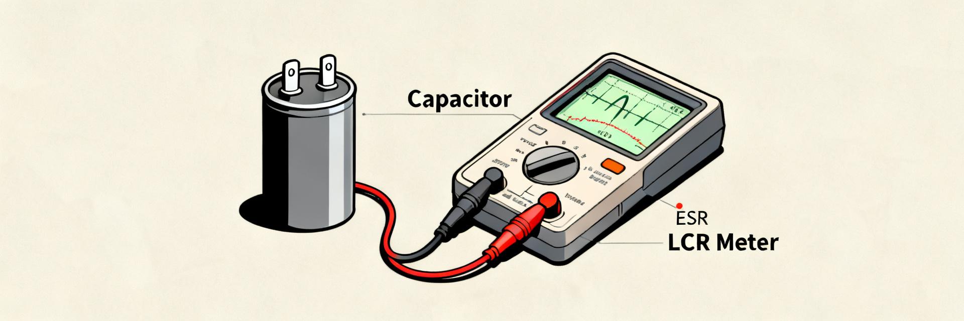
Explanation: Measure contact resistance with a 4-wire (Kelvin) setup using 100 mA–1 A test current per datasheet practice; expect values in the single-digit to tens of milliohms. Measure insulation resistance with a megohmmeter at the specified DC test voltage and time to verify ≥MΩ ratings.
Dielectric withstanding voltage and creepage/clearance considerations
Point: Dielectric test voltage defines isolation capability.
Evidence: The datasheet gives AC hipot values and duration (for example, 1000 VAC for 1 minute).
Explanation: Use the dielectric number to set PCB creepage/clearance: for a 250 VAC working voltage, target creepage/clearance per relevant safety standards (or conservatively 3–6 mm) and increase spacing when conformal coatings or elevated pollution degrees apply. Correlate the datasheet hipot to system-level isolation requirements during safety approval.
(4) Thermal behavior, derating curves & reliability drivers (method guide)
How to read or approximate derating curves from the datasheet
Point: Derating curves show allowable current vs. temperature.
Evidence: If a current-vs-temperature graph exists, it ties rated current to ambient and/or conductor rise.
Explanation: Reproduce curves by plotting rated current at the datasheet reference temperature, then apply conductor and bundle corrections (IPC-2152). If no curve exists, approximate derating: reduce rated current by ~10% per 10°C above 25°C or apply a 70% rule for continuous operation in constrained enclosures.
Materials, plating and long-term electrical stability
Point: Base metal and plating determine contact resistance drift.
Evidence: Datasheet notes list contact materials (e.g., phosphor bronze) and platings (tin/gold) plus any environmental notes.
Explanation: Choose gold plating for low-resistance, low-wear signal contacts; tin is acceptable for lower-cost power contacts but may show higher oxidation and resistance drift. Factor plating into maintenance intervals and life-cycle testing for long-term stability.
(5) Test & validation procedures you should run (method guide)
Reproducing datasheet tests in your lab
Point: Recreate datasheet test conditions to validate parts.
Evidence: Key tests include contact resistance (4-wire), dielectric withstanding voltage (AC hipot), insulation resistance (DC megohmmeter), and temperature cycling.
Explanation: Minimum steps—use 4-wire ohmmeter at datasheet current, perform AC hipot to listed voltage for specified time with proper trip limits, measure insulation resistance at the stated DC voltage, and run thermal cycling per datasheet cycles. Log test fixtures, torque, and wiring harness states to match datasheet conditions.
Troubleshooting common failures and interpreting deviations
Point: Distinguish connector issues from assembly defects.
Evidence: High contact resistance often correlates to plating wear, contamination, or under-torqued/poor solder joints.
Explanation: Diagnose by inspecting plating, repeating 4-wire measurements, and swapping mating parts. When readings deviate marginally from datasheet, treat as process variability; large deviations usually signal assembly or material defects requiring corrective action rather than component rejection alone.
(6) Design checklist, PCB implementation & comparable use-cases (action-focused)
PCB footprint, mechanical mounting and soldering notes
Point: Implement footprint per datasheet and verify solder constraints.
Evidence: Datasheet gives pad sizes, hole diameters, and soldering temperature limits/reflow profiles.
Explanation: Checklist items—copy pad and hole dimensions exactly, include keepouts for creepage, specify solder mask slivers to prevent bridging, and observe max reflow temperatures. Verify mechanical mounting keeps contact pressure even and that board-to-board spacing supports dielectric requirements.
Quick selection checklist & when to choose this part vs. alternatives
Point: Use a one-page decision checklist keyed to electrical specs and the datasheet.
Evidence: Compare voltage, current, temperature, contact resistance, and plating when evaluating alternatives.
Explanation: Choose this part when pitch, pin count, and rated current match system needs; select alternatives when higher continuous current, gold plating, or increased isolation spacing are required. Always validate selections against the datasheet and planned test conditions.
Key Summary
- 43045-1012 selection pivots on continuous current and dielectric test values; prioritize rated current and dielectric withstanding voltage when mapping to PCB trace sizing and isolation requirements, and apply conservative derating to account for ambient rise.
- Contact resistance and insulation resistance should be measured with 4-wire and megohmmeter setups under datasheet conditions; these values drive signal integrity and leakage considerations and must be retested post-assembly.
- Reproduce datasheet tests in lab fixtures—hipot, insulation, contact resistance, and thermal cycling—and use deviations to separate component issues from assembly/process faults; validate PCB creepage/clearance using the dielectric numbers.
Frequently Asked Questions
What does the 43045-1012 rated current mean for PCB trace sizing?
Rated current specifies the maximum current the connector pin is designed to carry continuously under defined ambient and contact temperature rise. For PCB traces, convert the pin rating into trace width using IPC-2152 tables, then apply a derating factor (commonly 70% for continuous thermal margin) and account for adjacent heat sources and via thermal resistance when finalizing trace geometry.
How should I test contact resistance for 43045-1012 in my lab?
Use a 4-wire (Kelvin) measurement with stable test current per datasheet (commonly 100 mA–1 A). Precondition samples if the datasheet specifies mating cycles, measure at multiple positions under defined contact force, and report the average milliohm value and any outliers. Ensure fixture contact surfaces match mating hardware to avoid measurement artifacts.
What dielectric withstanding voltage from the datasheet implies for PCB spacing?
The datasheet’s hipot voltage and duration indicate the connector’s isolation capability; translate that into PCB creepage/clearance targets based on working voltage and pollution degree. For conservative designs, choose spacing exceeding standard recommendations (e.g., several millimeters for mains-level voltages) and add conformal coating when space is limited or pollution degree is high.