RM06F84R5CT Resistencia 0603: Hoja de datos y huella para PCB
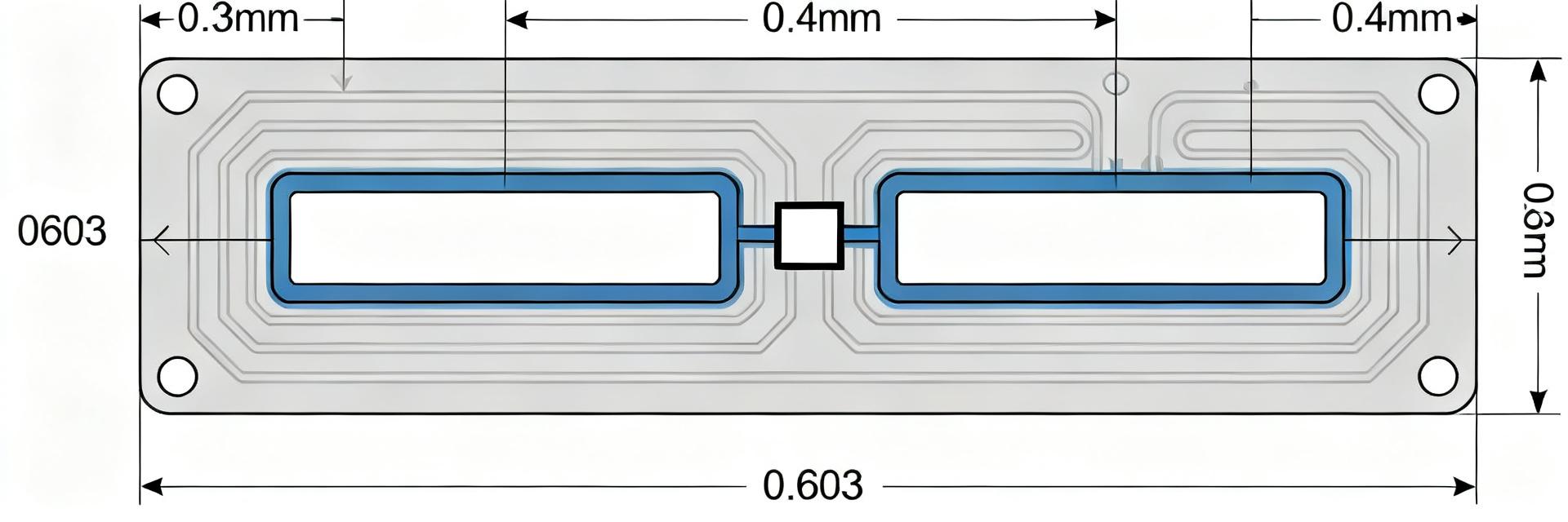
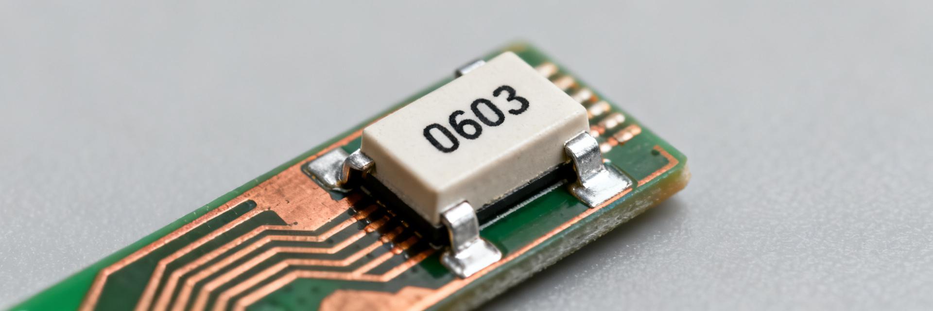
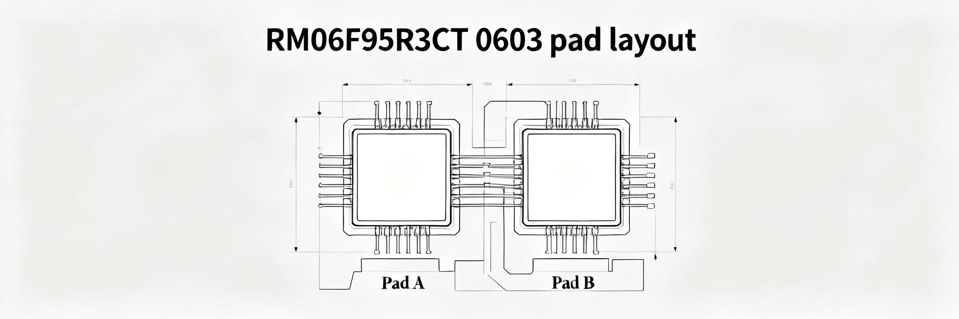
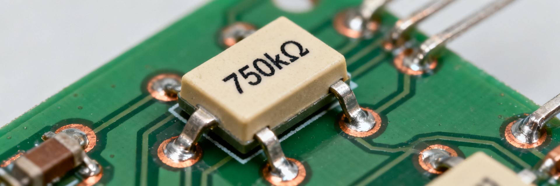
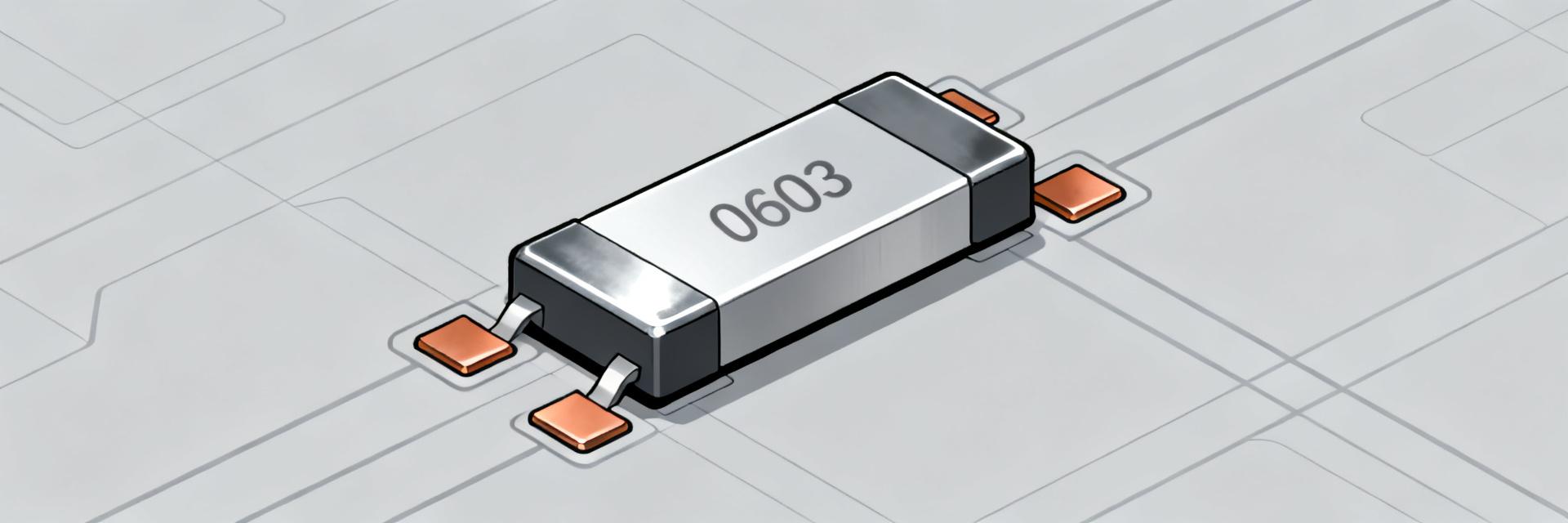
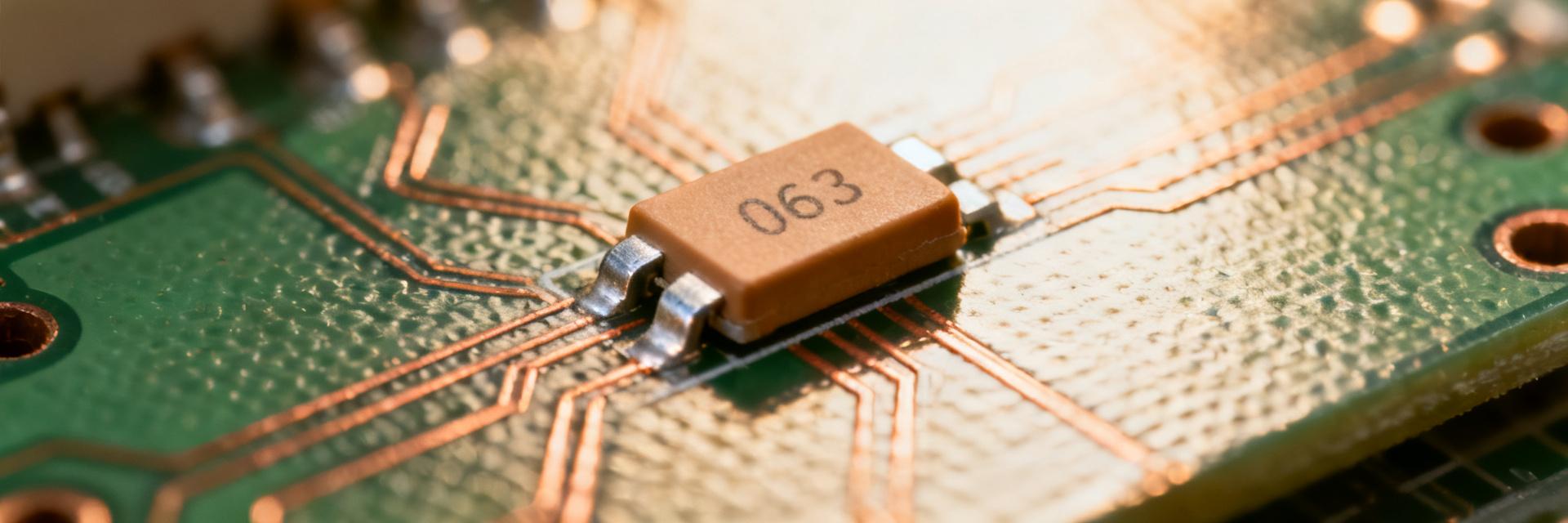
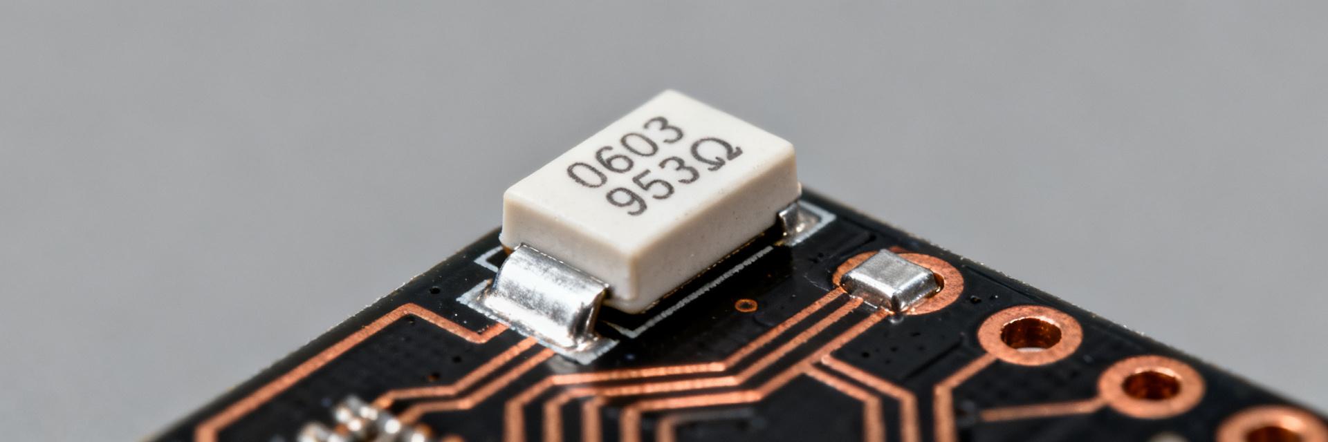
El RM06F84R5CT se especifica comúnmente donde el espacio de la placa es limitado y la confiabilidad es importante; los PCB modernos de alta densidad todavía utilizan el formato 0603 para diseños de señal mixta. Leer correctamente la hoja de datos del RM06F84R5CT y crear una huella de PCB compatible con IPC afecta directamente el rendimiento de la soldadura y la confiabilidad a largo plazo en el campo. Este artículo ofrece un resumen rápido de especificaciones, guía de huellas, consejos de ensamblaje y una lista de verificación práctica para diseñadores y ensambladores. Descripción general del producto: el RM06F84R5CT de un vistazo Identidad de la pieza y aplicaciones típicas El RM06F84R5CT se decodifica como un resistor de chip de película gruesa de la serie 0603 con un valor nominal indicado en el medio del código de pieza y clases de tolerancia estándar disponibles. Las aplicaciones típicas incluyen entradas de sensores, pull-ups e implementaciones compactas de detección de corriente donde el perfil bajo y el área mínima de la placa son prioridades. Confirme la tolerancia, la opción de TCR y el empaque (cinta y carrete) al agregar el RM06F84R5CT a una lista de materiales (BOM). Por qué el tamaño de la resistencia 0603 es importante para las PCB modernas La resistencia 0603 mide aproximadamente 0.06" × 0.03" (~1.6 × 0.8 mm), ofreciendo una excelente relación área-función para placas densas. El uso de una resistencia 0603 reduce la congestión de enrutamiento pero limita la disipación de potencia permitida y aumenta la sensibilidad de manejo. Las limitaciones del empaque influyen en las decisiones de huella, las opciones de alivio térmico y las herramientas de pick-and-place, por lo que los diseñadores deben sopesar el ahorro de espacio frente a los compromisos térmicos y de ensamblaje. PAD 1 (ENTRADA) PAD 2 (SALIDA) RM06F84R5CT (0603) Análisis profundo de la hoja de datos: especificaciones eléctricas, mecánicas y térmicas Especificación de parámetro Valor RM06F84R5CT Impacto en diseño y diseño de PCB Resistencia nominal 84.5 Ω (Decodificado mediante "84R5") Crítico para el emparejamiento de rutas directas y controles de impedancia Tolerancia estándar ±1.0% (Estándar Clase F) Establece límites precisos para interfaces analógicas de alto rendimiento Límite de disipación de potencia 0.1W (1/10 de vatio a 70°C) Requiere alivio térmico local y comprobaciones estrictas de potencia a área Coeficiente de temperatura (TCR) ±100 ppm/°C Minimiza la deriva sobre rangos de temperatura operativos estándar Especificaciones eléctricas a verificar (qué extraer de la hoja de datos) Campos eléctricos clave a extraer: resistencia nominal, tolerancia, potencia nominal (con condiciones de montaje en PCB), coeficiente de temperatura de la resistencia (TCR), corriente nominal y límites de sobretensión, factor de ruido y energía de pulso permitida. También capture curvas de reducción de potencia (derating) o gráficos que muestren la potencia frente a la temperatura ambiente y cualquier temperatura máxima especificada del punto caliente para evitar sobreesfuerzos en la aplicación. Parámetros mecánicos y térmicos que afectan la huella/diseño A partir de la hoja de datos, registre las dimensiones del componente, la geometría de la terminación, los máximos recomendados de soldadura y los límites del perfil de reflujo. Tenga en cuenta las condiciones recomendadas de almacenamiento y manipulación. Si el proveedor proporciona un patrón de tierra recomendado, registre esas dimensiones; de lo contrario, registre la temperatura máxima de soldadura y el tiempo de pico sugerido para guiar las decisiones de esténcil y pad durante el diseño. Recomendaciones de huella de PCB y patrón de tierra para 0603 Patrón de tierra guiado por IPC - dimensiones recomendadas de pad (ejemplo práctico) Siga la guía de IPC-7351 para patrones de tierra SMD y valídela con el fabricante. Ejemplo de tamaño nominal de componente: ~0.06" × 0.03" (≈1.6 × 0.8 mm). Un ejemplo práctico de patrón de tierra utiliza longitudes de pad de aproximadamente 0.9 mm y anchos de pad cercanos a 0.6 mm con un espacio entre pads de alrededor de 0.1–0.2 mm; adapte estos rangos para pads definidos por máscara de soldadura frente a pads definidos por cobre. Siempre verifique la huella de PCB contra la hoja de datos de la pieza y la capacidad del ensamblador. Recomendaciones de máscara de soldadura, esténcil y pasta para minimizar defectos Utilice una cobertura de pasta del 60–80% por pad como punto de partida y formas de apertura comunes (rectangulares con esquinas redondeadas) para controlar la humectación. El espesor típico del esténcil es de 0.10–0.15 mm (4–6 mil); reduzca el área de la abertura de un 10 a un 30% para resistencias delgadas para reducir el riesgo de efecto lápida. Considere pasta asimétrica para terminaciones de disipación de calor cuando un extremo tiene una mayor masa térmica para equilibrar las fuerzas de soldadura durante el reflujo. Consideraciones de ensamblaje y confiabilidad (reflujo, inspección, modos de falla) Perfiles de reflujo y mejores prácticas de soldadura para resistencias 0603 Adopte un perfil de reflujo sin plomo que respete la temperatura máxima de soldadura del componente: una rampa controlada (~1–3 °C/s), una zona de mantenimiento (soak) para activar el flux y un tiempo pico dentro de los límites del proveedor (lo suficientemente corto como para evitar el sobreesfuerzo). Ajuste el tamaño de la boquilla de pick-and-place y la velocidad de colocación para minimizar la vibración y reducir la desalineación; ajuste la fuerza de colocación para evitar que el componente se incline en piezas 0603. Modos de falla comunes y recomendaciones de prueba/inspección Las fallas frecuentes incluyen efecto lápida, filetes de soldadura incompletos, agrietamiento mecánico y sobreesfuerzo electrotérmico. Inspeccione con microscopía óptica para evaluar la calidad del filete y rayos X para encontrar vacíos ocultos en PCB de alta densidad. Realice pruebas de confiabilidad específicas, como ciclos térmicos, choques mecánicos y congelación por humedad según la guía IPC para la calificación. Defina criterios de aceptación para la creación de prototipos frente a la producción para agilizar el triaje de fallas. Lista de verificación de implementación y notas de producción/BOM Lista de verificación de diseño a producción (pasos prácticos) Antes del lanzamiento: confirme los valores eléctricos y térmicos de la hoja de datos, finalice una huella compatible con IPC, ejecute comprobaciones de DRC y DFM, genere un modelo 3D, verifique las aberturas del esténcil, cree prototipos con el proveedor de ensamblaje previsto y realice pruebas térmicas y funcionales. También valide los programas de colocación y la configuración de reflujo en una serie piloto antes de comprometerse con la producción en volumen para detectar sorpresas térmicas o de ensamblaje de manera anticipada. Nombramiento en BOM, adquisición y detalles de pick-and-place Enumere el formato exacto del número de pieza en la BOM para evitar sustituciones y observe la orientación de la cinta y el carrete y la cantidad del carrete. Proporcione la orientación del alimentador y el tipo de boquilla preferido en las notas de ensamblaje (boquilla de vacío pequeña de ~0.8–1.0 mm típica). Incluya convenciones de designadores de referencia y cualquier alternativa prohibida para mantener la coherencia de la adquisición y la colocación en todas las compilaciones. Resumen (conclusión) Verifique los campos críticos de la hoja de datos (resistencia, tolerancia, clasificación de potencia, TCR y curvas de reducción de potencia) antes de finalizar la colocación y el diseño térmico para evitar el sobreesfuerzo del RM06F84R5CT en diseños densos. Siga la geometría de pad informada por IPC para la resistencia 0603 y valide la huella de PCB y las opciones de máscara de soldadura con su ensamblador para reducir el efecto lápida y los defectos de soldadura. Ejecute un piloto controlado: finalice las aberturas de esténcil, ajuste los programas de reflujo y pick-and-place, inspeccione con métodos ópticos/rayos X y realice pruebas térmicas/mecánicas específicas antes de las series de volumen. Valide la huella final contra la hoja de datos del componente y su ensamblador por contrato antes de la producción en volumen. Preguntas comunes ¿Cómo decodifico el número de pieza RM06F84R5CT? El número de pieza se decodifica de la siguiente manera: RM representa la serie de resistencias de chip de película gruesa, 06 denota la escala de empaque métrico 0603 (1608), F especifica la clase de tolerancia de precisión del 1%, 84R5 denota el valor de resistencia nominal de 84.5 ohmios y CT se refiere al empaque estándar de cinta de papel y carrete (Paper Tape & Reel). ¿Cómo confirmo los valores correctos de la hoja de datos para esta resistencia? Comience por extraer la resistencia nominal, la tolerancia, la potencia nominal, el TCR y la temperatura máxima de soldadura. Verifique las curvas de reducción de potencia (derating) y los límites de sobretensión de pulso/corriente; registre el patrón de tierra recomendado si se proporciona. Compare estos valores con su modelo térmico y las limitaciones de pick-and-place antes de aprobar la BOM para adquisición. ¿Qué problemas de huella de PCB causan comúnmente fallas de ensamblaje? Los problemas comunes incluyen aberturas de esténcil de pasta sobredimensionadas, pads que no tienen en cuenta la tolerancia del componente y una holgura inadecuada de la máscara de soldadura. Esto provoca efecto lápida, puentes de soldadura o filetes insuficientes. Utilice la guía IPC, valide un esténcil de muestra y ejecute una prueba piloto rápida de colocación y reflujo para confirmar que la huella elegida funcione de manera confiable en el apilamiento de capas de su placa. ¿Qué pasos de inspección y prueba son esenciales para las primeras series de producción? Realice una inspección óptica de los filetes de soldadura, seleccione rayos X en placas densas para encontrar vacíos ocultos y realice ciclos térmicos simples y pruebas funcionales en prototipos. Defina criterios de aceptación (continuidad eléctrica, sin grietas visibles, resistencia estable a lo largo de los ciclos) para detectar problemas marginales de ensamblaje antes de escalar a una producción mayor.