RM06F84R5CT 0603 Resistor: Datasheet & PCB Footprint
The RM06F84R5CT is commonly specified where board real estate is constrained and reliability matters; modern high-density PCBs still use the 0603 form-factor for mixed-signal designs. Correctly reading the RM06F84R5CT datasheet and creating an IPC-aware PCB footprint directly impacts solder yield and long-term field reliability. This article gives quick spec highlights, footprint guidance, assembly tips, and a practical checklist for designers and assemblers.
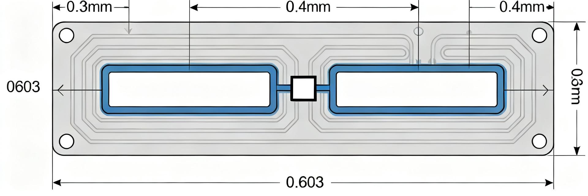
Product overview — RM06F84R5CT at a glance
Part identity & typical applications
RM06F84R5CT decodes as a 0603-series thick-film chip resistor with a nominal value indicated in the middle of the part code and standard tolerance classes available. Typical applications include sensor inputs, pull-ups, and compact current-sense implementations where low profile and minimal board area are priorities. Confirm tolerance, TCR option, and packaging (tape & reel) when adding RM06F84R5CT to a BOM.
Why 0603 resistor size matters for modern PCBs
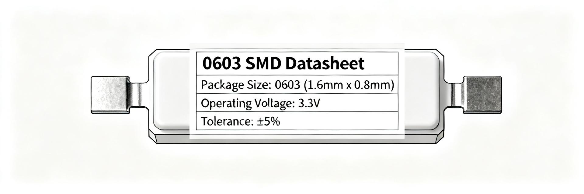
The 0603 resistor measures roughly 0.06" × 0.03" (~1.6 × 0.8 mm), offering a strong area-to-function ratio for dense boards. Using a 0603 resistor reduces routing congestion but limits allowable power dissipation and increases handling sensitivity. Package constraints influence footprint decisions, thermal relief choices, and pick-and-place tooling, so designers must weigh space savings against assembly and thermal trade-offs.
Datasheet deep-dive — electrical, mechanical & thermal specs
| Parameter Specification | RM06F84R5CT Value | PCB Design & Layout Impact |
|---|---|---|
| Nominal Resistance | 84.5 Ω (Decoded via "84R5") | Critical for direct path matching & impedance controls |
| Standard Tolerance | ±1.0% (Class F standard) | Establishes precise bounds for high-performance analog interfaces |
| Power Dissipation Limit | 0.1W (1/10 Watt at 70°C) | Requires local thermal relief & strict power-to-area checks |
| Temperature Coefficient (TCR) | ±100 ppm/°C | Minimizes drift over standard operational temperature bands |
Electrical specifications to check (what to extract from the datasheet)
Key electrical fields to extract: nominal resistance, tolerance, rated power (with PCB mounting conditions), temperature coefficient of resistance (TCR), rated current and surge limits, noise figure, and allowable pulse energy. Also capture derating curves or charts showing power versus ambient temperature and any specified maximum hot-spot temperature to avoid overstress in application.
Mechanical & thermal parameters that affect footprint/layout
From the datasheet record component dimensions, termination geometry, recommended soldering maximums, and reflow profile limits. Note recommended storage and handling conditions. If the vendor provides a recommended land pattern, capture those dimensions; otherwise record maximum solder temperature and suggested peak time to guide stencil and pad decisions during layout.
PCB footprint & land-pattern recommendations for 0603
IPC-guided land pattern — recommended pad dimensions (practical example)
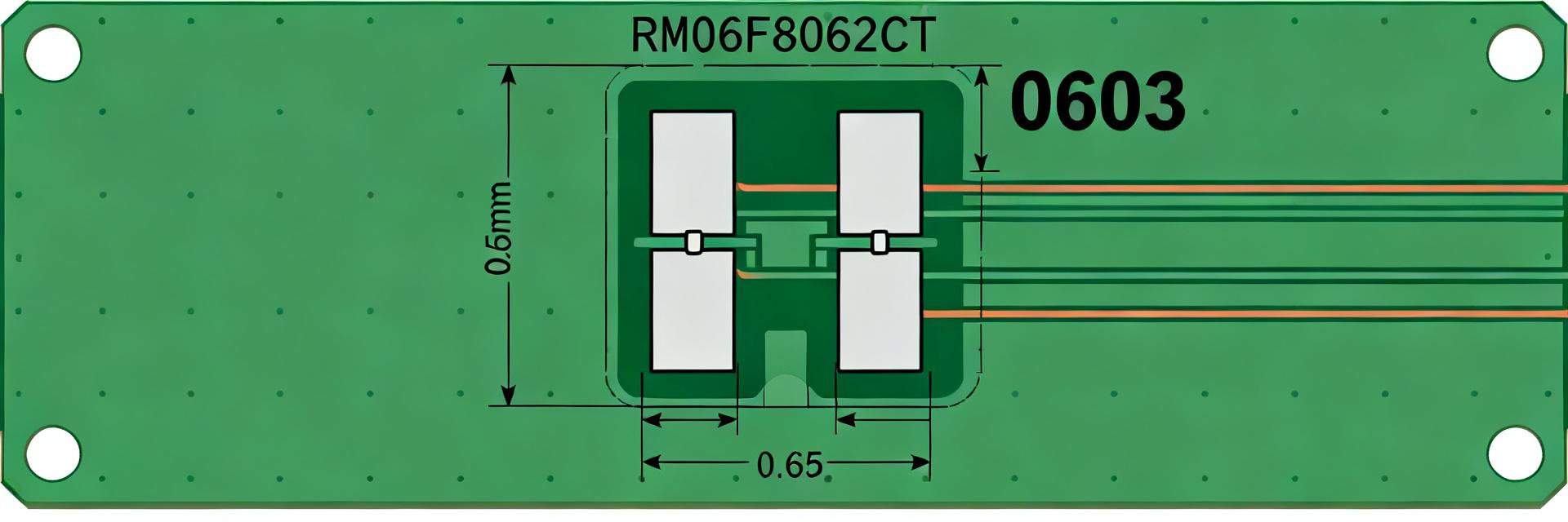
Follow IPC-7351 guidance for SMD land patterns and validate against the manufacturer. Example nominal component size: ~0.06" × 0.03" (≈1.6 × 0.8 mm). A practical example land pattern uses pad lengths of about 0.9 mm and pad widths near 0.6 mm with a pad-to-pad gap around 0.1–0.2 mm; adapt these ranges for soldermask-defined versus copper-defined pads. Always verify the PCB footprint against the part datasheet and assembler capability.
Solder mask, stencil and paste recommendations to minimize defects
Use 60–80% paste coverage per pad as a starting point and common aperture shapes (rectangular with rounded corners) to control wetting. Typical stencil thickness is 0.10–0.15 mm (4–6 mil); reduce aperture area 10–30% for thin resistors to reduce tombstoning risk. Consider asymmetric paste for heat-sinking terminations when one end has higher thermal mass to balance solder forces during reflow.
Assembly & reliability considerations (reflow, inspection, failure modes)
Reflow profiles and soldering best practices for 0603 resistors
Adopt a lead-free reflow profile that respects the component maximum solder temperature: a controlled ramp (~1–3 °C/s), a soak region to activate flux, and a peak time within vendor limits (short enough to avoid overstress). Tune pick-and-place nozzle size and placement speed to minimize vibration and reduce misplacement; fine-tune placement force to prevent component tilting for 0603 parts.
Common failure modes and test/inspection recommendations
Frequent failures include tombstoning, incomplete solder fillets, mechanical cracking, and electrothermal overstress. Inspect with optical microscopy for fillet quality and X‑ray for hidden voids on densified PCBs. Run targeted reliability tests such as thermal cycling, mechanical shock, and humidity‑freeze per IPC guidance for qualification. Define acceptance criteria for prototyping versus production to streamline failure triage.
Implementation checklist & BOM / production notes
Design-to-production checklist (actionable steps)
Before release: confirm datasheet electrical and thermal values, finalize an IPC-aware footprint, run DRC and DFM checks, generate a 3D model, verify stencil apertures, prototype with intended assembly vendor, and run thermal and functional tests. Also validate placement programs and reflow settings in a pilot run before committing to volume production to catch assembly or thermal surprises early.
BOM naming, procurement and pick-and-place details
List the exact part number formatting in the BOM to avoid substitutions and note tape-and-reel orientation and reel quantity. Provide feeder orientation and preferred nozzle type in assembly notes (small vacuum nozzle ~0.8–1.0 mm typical). Include reference designator conventions and any forbidden alternates to keep procurement and placement consistent across builds.
Summary (conclusion)
- Verify datasheet critical fields—resistance, tolerance, power rating, TCR and derating curves—before finalizing placement and thermal design to prevent overstress of RM06F84R5CT in dense layouts.
- Follow IPC-informed pad geometry for the 0603 resistor and validate the PCB footprint and soldermask choices with your assembler to reduce tombstoning and solder defects.
- Run a controlled pilot: finalize stencil apertures, tune reflow and pick‑and‑place programs, inspect with optical/X‑ray methods, and perform targeted thermal/mechanical tests prior to volume runs.
Validate the final footprint against the component datasheet and your contract assembler before volume production.
Common questions
How do I decode the RM06F84R5CT part number?
The part number decodes as follows: RM represents Thick Film Chip Resistor series, 06 denotes the 0603 metric packaging scale (1608), F specifies the 1% precision tolerance class, 84R5 denotes the nominal resistance value of 84.5 Ohms, and CT refers to standard Paper Tape & Reel packaging.
How do I confirm the correct datasheet values for this resistor?
Start by extracting nominal resistance, tolerance, rated power, TCR, and maximum soldering temperature. Check for derating curves and pulse/current surge limits; record recommended land pattern if provided. Cross‑reference these values with your thermal model and pick‑and‑place constraints before approving the BOM for procurement.
What PCB footprint issues commonly cause assembly failures?
Common issues include oversized paste apertures, pads that do not account for component tolerance, and inadequate soldermask clearance. These lead to tombstoning, bridging, or insufficient fillets. Use IPC guidance, validate a sample stencil, and run a quick placement and reflow pilot to confirm the chosen footprint performs reliably on your board stackup.
Which inspection and test steps are essential for early production runs?
Perform optical inspection for solder fillets, select X‑ray on dense boards to find hidden voids, and run simple thermal cycling and functional tests on prototypes. Define acceptance criteria (electrical continuity, no visible cracks, stable resistance across cycles) to catch marginal assembly issues before scaling to larger production.