0603 976Ω SMD Resistor: Full Specs & Notes for PCB Design
Recent component-usage surveys show that 0603 chip resistors remain a top choice across consumer and industrial PCBs because they balance board area and electrical performance. The 0603 976Ω value is commonly used in signal paths, pull networks, and RC filters where a sub‑1 kΩ value better matches tolerance and time constant targets. This introduction frames how to translate datasheet specs into PCB rules so designers can pick, place, and validate the part with confidence; all numeric ranges are typical—verify on manufacturer datasheet.
The following guide treats the 0603 976Ω as a standard SMD resistor case study, focusing on package interpretation, electrical specs, footprint and soldering practices, thermal and reliability considerations, and a compact design checklist. Practical tradeoffs—tolerance versus cost, thick‑film versus metal‑film for noise and TCR—are highlighted so designers can make data‑driven choices and avoid common assembly pitfalls.
Background: What "0603 976Ω" Means and Where It Fits

Package code & physical dimensions
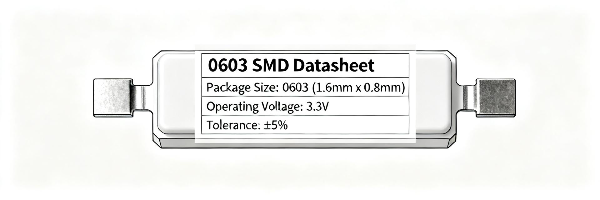
“0603” is an imperial package code that denotes roughly 0.060" × 0.030" (approx. 1.6 mm × 0.8 mm) footprint; manufacturing tolerances on length/width/thickness affect pick‑and‑place and fillet formation. Smaller tolerances can reduce solder fillet volume and change wetting behavior, so land pattern pad length is typically tuned to promote a proper toe and heel fillet. Marking schemes are minimal on 0603 parts; three‑ or four‑digit codes map to resistance values per standard resistor coding conventions.
Typical applications for a 976Ω value
A 976Ω resistor often appears as pull‑ups/pull‑downs, bias resistors in amplifier networks, and the R portion of RC filters where a slightly lower than 1 kΩ value compensates for tolerance or loading. Designers choose 976Ω versus a nominal 1 kΩ to align with E‑series availability, tolerance chains, or to meet precise time constants without changing capacitor values. It is a common SMD resistor choice in signal and control circuits due to that flexibility.
Full Electrical Specs for 0603 976Ω (key specs & implications)
Resistance tolerance, E‑series & marking interpretation
Common tolerances for 0603 resistors include ±5% (E24), ±1% (E96), and ±0.1% for precision thin‑film devices; choose tolerance based on noise, calibration, and cost tradeoffs. A 976Ω value typically maps directly in E96 or is a standard trimmed value in precision families. When specifying a tolerance, consider system calibration steps and whether resistor network matching or absolute accuracy is critical; tighter tolerance increases cost and may require thin‑film parts (typical—verify on manufacturer datasheet).
Power rating, voltage rating, TCR, and noise
Typical 0603 power ratings on a standard FR‑4 PCB with modest copper are around 0.06–0.10 W; peak working voltages for many thick‑film chips are ~50 V, and TCR ranges span several hundred ppm/°C for thick film versus 5–50 ppm/°C for metal film. Noise and parasitic L/C are higher in thick‑film parts; for low‑noise or high‑speed circuits choose metal‑film or specialized low‑noise types. All numerical ranges are typical—verify on manufacturer datasheet.
| Spec | Typical range (0603) | Design note |
|---|---|---|
| Power rating | 0.06–0.10 W | Derate for large copper planes (use thermal rules) |
| TCR | ~5–300 ppm/°C | Use metal‑film for ppm <50 |
| Working voltage | ~50–200 V (part dependent) | Check peak and surge specs on datasheet |
PCB Footprint, Placement & Soldering Notes for 0603 976Ω SMD Resistor
Recommended land pattern & pad dimensions
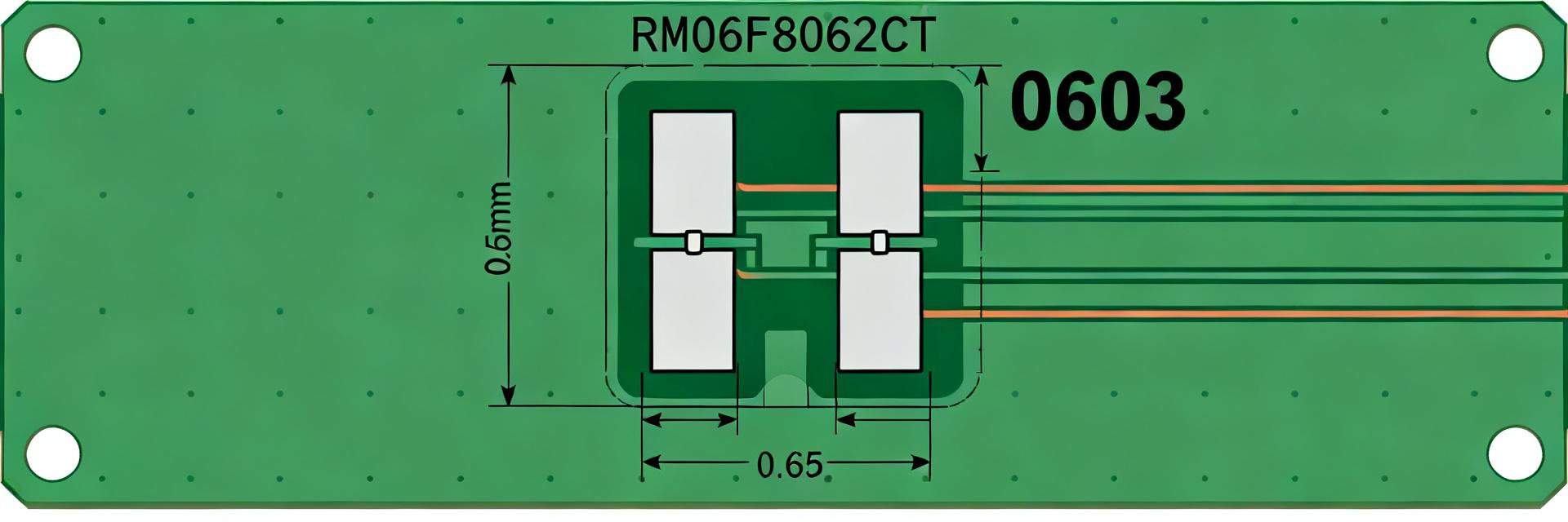
Start with a land pattern of ≈1.0–1.2 mm pad length and 0.6–0.7 mm pad width for 0603 as a baseline; adjust toe/heel spacing per fab and assembler preferences to achieve reliable solder fillets. Include solder mask openings slightly smaller than pads to control wetting. Pick‑and‑place alignment tolerance is typically ±0.05 mm; add nearby fiducials for dense boards to keep placement accuracy high.
Reflow, stencil & tombstoning mitigation
Use stencil apertures that cover 60–80% of the pad area as a starting point; paste thickness around 0.12–0.15 mm works for 0603 on standard processes. A controlled reflow with a moderate ramp and peak near common lead‑free profiles (typical peak 235–250°C) reduces voiding—typical—verify on manufacturer datasheet. To reduce tombstoning, keep paste proportion symmetric, avoid single‑sided heavy paste, and place thermally similar neighbors or add copper heat sinks to balance wetting forces.
Thermal, Reliability & Test Considerations
Thermal derating and PCB copper influence
Copper plane area and thermal vias change the effective dissipation of a 0603 resistor: a large copper pour can sink heat and lower the steady‑state surface temperature, permitting higher continuous power before derating. As a rule of thumb, derate nominal part power by 20–50% when pads are connected to significant copper; run thermal simulation checkpoints and measure prototype surface temperature rise at representative power levels (typical—verify on manufacturer datasheet).
Reliability: solder fatigue, humidity, shock & testing
Common failure modes include solder fatigue from CTE mismatches, resistor body cracking from mechanical shock, and resistance drift under prolonged humidity exposure. Recommended qualification steps: thermal cycling, humidity soak, mechanical vibration, and periodic electrical stability checks. For cleaning, avoid aggressive solvents that can attack certain passivation layers; validate cleaning agents on sample boards.
Practical Design Checklist & Example Use Cases (actionable)
Quick PCB designer checklist
Action items: confirm tolerance and TCR requirements; derate 0603 power based on pad copper (20–50% rule of thumb); set footprint to recommended pad dimensions; specify stencil % (60–80%); plan part orientation for pick‑and‑place; include test points for critical nodes. Also document whether thick‑film or metal‑film is required and note “typical—verify on manufacturer datasheet” next to electrical limits in the BOM.
Two concise example scenarios
Example A — Microcontroller pull‑up: choose ±1% if ADC sampling or threshold precision matters, otherwise ±5% for general GPIO. Expect negligible dissipation when used as pull‑up to 3.3 V; place resistor within 1–2 mm of MCU pin to minimize trace stray inductance. Example B — RC filter: using 976Ω with a 100 nF cap yields ~1.63 kHz cutoff; prefer metal‑film if filter Q and stability are critical, and keep traces short to minimize parasitic capacitance and preserve time constant accuracy.
Summary
Choosing the right 0603 976Ω component requires matching tolerance, family, and PCB thermal context to the application. Derate 0603 parts for copper plane effects, use recommended land patterns to ensure reliable fillets, adopt balanced stencil and reflow practices to reduce tombstoning, and validate with thermal and reliability testing. For sensitive circuits, prefer metal‑film for low TCR and noise; for economy choose thick‑film with appropriate tolerance. All numeric guidelines are typical—verify on manufacturer datasheet.
- Specify tolerance and TCR early: tighter tolerances (±1% or ±0.1%) and lower TCR improve accuracy but increase cost; note this when ordering 0603 parts.
- Derate for copper: reduce assumed continuous power by 20–50% for parts tied to large copper pours or planes to avoid overheating.
- Footprint and stencil: start with 1.0–1.2 mm pad length and 60–80% stencil aperture; adjust per assembler feedback to ensure consistent fillets and paste volume.
FAQ
How should I size the 0603 976Ω footprint for my PCB?
Use a baseline pad length of 1.0–1.2 mm and pad width of 0.6–0.7 mm, then confirm with your assembler. These pads promote a reliable toe and heel fillet while keeping solder volume manageable; adjust the solder mask aperture to control wetting. Always prototype and inspect fillets under representative reflow conditions (typical—verify on manufacturer datasheet).
What power derating should I apply to a 0603 976Ω on a copper plane?
Derate nominal 0603 power by roughly 20–50% when pads tie into large copper areas or thermal planes. The exact derating depends on copper area, number of thermal vias, and board stackup; run a quick thermal simulation or measure temperature rise on a prototype at expected steady‑state dissipation to set safe continuous power limits (typical—verify on manufacturer datasheet).
Is 0603 976Ω suitable for low‑noise analog circuits?
Use metal‑film 0603 resistors for low‑noise analog paths, as thick‑film types can exhibit higher excess noise and larger TCR. If noise floor or matching is critical, specify low‑noise or precision thin‑film resistors and include them in your BOM notes. Also consider board layout: keep resistor‑to‑amplifier traces short and minimize coupling to switching nodes.
What are the key differences between thick-film and metal-film 0603 976Ω resistors?
Thick-film resistors are cost-effective but feature higher TCR (typically ~100-300 ppm/°C) and higher noise. Metal-film (thin-film) resistors offer superior accuracy (down to 0.1%), lower TCR (5-50 ppm/°C), and significantly lower current noise, making them ideal for high-precision instrumentation and filtering.