• 26-01-3114 사양 심층 분석: 피치, 마운트 및 핀아웃 설명

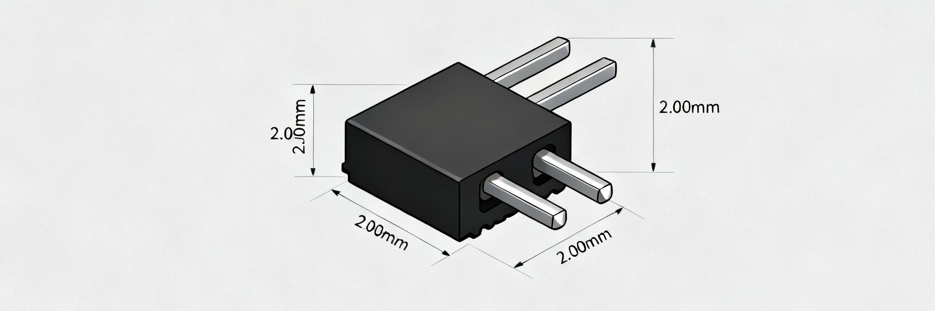
    The 26-01-3114 is a precision-engineered dual-row, right-angle through-hole PCB header. Recognized by its 4.2 mm (0.165 in) pitch, this component is a staple in industrial power and signal distribution. Mismatches in mounting or pin mapping are leading causes of board re-spins; this technical breakdown ensures your layout is accurate from the first iteration. ParameterSpecificationImpact on Design In-Row Pitch4.2 mm (0.165")Determines grid and pad spacing Mounting StyleRight-Angle T/HDictates edge clearance and keepouts Row ConfigurationDual-Row OffsetAffects trace routing complexity Tail LengthShort ProfileRequires precise drill/plating tolerances 1 — Mechanical Specs: Pitch and Dimensions The 4.2 mm pitch refers to the center-to-center distance between adjacent pins in a single row. For the 26-01-3114, designers must account for both the in-row pitch and the row-to-row spacing, which are independent datums in most professional datasheets. A placement tolerance of ±0.1 mm is standard for automated assembly. PIN 1 PIN 2 PIN 3 4.2mm Pitch BODY (R/A) 2 — Mounting & PCB Footprint Guide Reliable through-hole joints depend on the relationship between the pin tail and the plated through-hole (PTH). For the 26-01-3114, use a drill size that provides a nominal +0.20 mm clearance. Annular rings should be sized to accommodate the current load while maintaining a minimum of 0.25 mm width to prevent breakout during thermal cycling. 3 — Pinout & Electrical Considerations Dual-row right-angle headers follow a specific numbering sequence. It is critical to pair the top-down PCB view with the schematic symbol. Document the orientation of the "Pin 1" indicator on the silkscreen. Electrical limits, such as the current rating per circuit and contact plating (typically Tin or Gold flash), must be cross-referenced with your trace width calculations to avoid overheating. 4 — Assembly & Troubleshooting IssueCauseFix Mating FailureWrong row spacingCorrect land pattern offset Weak Solder JointShort tail insertionAdjust wave profile / Hole size Housing TiltMissing locator pegsVerify peg-to-hole alignment How should designers verify the 26-01-3114 pitch and row spacing? Cross-reference the datasheet mechanical drawing with a 4.2 mm in-row pitch and implement in CAD with ±0.1 mm placement tolerance before running DRC against mechanical keepouts. What drill and pad sizes are recommended for right-angle tails? Use a drill equal to the nominal tail diameter plus 0.15–0.25 mm. Ensure annular rings are at least 0.25 mm. Use thermal reliefs for wave soldering to prevent cold joints. Which BOM fields prevent incorrect substitutions for headers? Specify the exact part number, 4.2 mm pitch, right-angle mounting, tail length, and plating material. Mention "with pegs" if mechanical alignment features are required. What are common assembly failures for 26-01-3114? Failures include misaligned pads preventing insertion, insufficient fillets on short tails, and interference with adjacent tall components due to the right-angle body overhang.
  • 26-01-3114 사양 심층 분석: 피치, 마운트 및 핀아웃 설명

    The 26-01-3114 is widely listed in datasheet and distributor summaries as a dual-row, right-angle through-hole PCB header with a 4.2 mm (0.165 in) in‑row pitch and short tails; small mismatches in pitch, mounting or pin mapping are a common root cause of board re-spins and assembly delays. This brief, data-led guide explains pitch, mount style and pinout in practical terms so designers can pick, footprint and assemble the part without surprises. References below assume checking the official datasheet and distributor listings for exact tolerances; the discussion uses those public specs generically to illustrate footprint, mechanical clearance and BOM fields designers should verify before layout sign-off. 1 — Background: What the 26-01-3114 is and why details matter 1.1 Key identifier summary Point: The part is a dual-row right-angle through-hole header commonly furnished in low pin-count variants. Evidence: distributor and datasheet summaries consistently list a 4.2 mm in‑row pitch, two offset rows, and short right-angle tails. Explanation: That form factor dictates board hole sizes, row spacing and keepouts; plating and material notes from listings guide solderability and current capacity decisions. 1.2 Why pitch, mount and pinout drive PCB success Point: Incorrect pitch, mounting angle or pin mapping causes mechanical interference and poor solder joints. Evidence: common failure modes recorded in assembly logs include misaligned pads and insufficient tail engagement. Explanation: A 0.1 mm pad offset can prevent full tail insertion, and a short tail length reduces available fillet area, so strict footprint and pinout checks prevent rework and delays. 2 — Mechanical specs deep-dive: Pitch, row spacing, and physical dimensions 2.1 Pitch explained (what 4.2 mm means for layout) Point: Pitch equals center‑to‑center spacing between pins; for this dual-row header the in‑row pitch is 4.2 mm (0.165 in) and row‑to‑row spacing is an independent datum. Evidence: distributor/datasheet summaries define both dimensions separately. Explanation: Layout must use a grid matching the 4.2 mm in‑row spacing, with row offset accounted for; recommended land pattern tolerances include ±0.1 mm pad placement and annular rings sized for the intended drill. 2.2 Other critical mechanical dims (tail length, peg/locator, mounting angle) Point: Tail length, any plastic locator pegs and the right‑angle body profile determine board clearance and mechanical retention. Evidence: mechanical drawings in listings show short tails that require full through‑hole insertion and pegs that align to dedicated holes. Explanation: Account for tail protrusion in side profiles, reserve keepout under the right‑angle body, and verify peg hole locations to avoid obstruction of nearby components. 3 — Mounting & PCB footprint guide (practical how-to) 3.1 Footprint rules: pads, thermal reliefs and drill sizes Point: Reliable through‑hole solder joints start with correct pad and drill specs. Evidence: common footprint recommendations from datasheets call for drilled holes sized to the nominal tail diameter plus plating and tolerance, with annular rings of at least 0.25 mm. Explanation: Use a drill that yields a snug tail fit (nominal +0.15–0.25 mm), define pad diameters to allow consistent fillets, and add thermal reliefs when wave soldering to control heat flow and avoid tombstoning on right‑angle tails. 3.2 Board layout tips: keepouts, mechanical reinforcement, and silkscreen Point: Keepouts and reinforcement avoid mechanical stress and mating interference. Evidence: assembly reports commonly flag adjacent tall components as interference with right‑angle connectors. Explanation: Specify a keepout matching the connector body footprint, include through‑hole pegs or glued rivets for mechanical loads, and add clear silkscreen markers for pin‑1 and mating orientation to speed assembly and inspection. 4 — Pinout & electrical considerations 4.1 Pin mapping and communication Point: Dual‑row right‑angle headers follow a defined numbering sequence—document it visually. Evidence: best practice schematics pair a top‑down PCB view with numbered pins. Explanation: Provide a top view diagram and BOM notes indicating pin 1 location. The 26-01-3114 should be called out by part number and pin map in both schematic and PCB fabrication outputs. 4.2 Electrical specs that matter Point: Electrical limits shape trace widths and reliability. Evidence: datasheet sections list rated current per pin and contact plating. Explanation: Use rated current to set trace width, confirm plating for solderability, and note contact area for low‑resistance connections; document these details in the BOM. 5 — Assembly, soldering & test: avoiding common failures 5.1 Soldering best practices Point: Solder process choice affects fillet quality and mechanical strength. Evidence: assembly records show consistent fillets with controlled wave parameters or careful hand soldering for short tails. Explanation: For wave soldering, set conveyor speed and preheat to allow full fillet formation on right‑angle tails; for manual soldering, aim for consistent wetting and avoid excessive solder that can bridge rows. 5.2 Test and validation checklist Point: A short QA checklist prevents escapes to test. Evidence: proven checklists include footprint verification, mechanical clearance, continuity and mating trials. Explanation: Pre‑assembly verify footprint dimensions; post‑assembly run continuity, solder fillet inspection and a mating test; document results and include pull‑test steps. 6 — Procurement & BOM tips + troubleshooting 6.1 What to specify: Specify full part number, pitch (4.2 mm), mounting angle, tail length, plating, and peg features in the BOM to match mechanical and electrical expectations for the 26-01-3114. 6.2 Quick troubleshooting: seven common issues and fixes Issue Cause Diagnosis Fix Misaligned mating housing Wrong row spacing Failed mating test Update row‑to‑row offset in footprint Insufficient solder fillet Short tail / wrong hole size Visual/AXI inspection Increase hole tolerance, adjust wave profile Poor mechanical retention No pegs or reinforcement Pull test fail Add peg holes, adhesive or rivets Summary Verify the 4.2 mm pitch and row spacing in your footprint to prevent mating and alignment errors; document pitch and mounting style in schematics and the BOM for clarity. Design the footprint for right‑angle tails: correct drill, pad sizes and keepouts, and include peg holes or reinforcement to handle mechanical loads and solder process variations. Document pinout unambiguously with a top‑down PCB pin diagram, and include electrical limits (current rating, plating) so trace widths and procurement match the connector’s capability. FAQ How should designers verify the 26-01-3114 pitch and row spacing before layout? Designers should cross‑reference the datasheet mechanical drawing and distributor dimensional summaries, confirm the 4.2 mm in‑row pitch and the specified row‑to‑row offset, then implement those values in CAD with a ±0.1 mm placement tolerance and run DRC against mechanical keepouts before releasing gerbers. What drill and pad sizes are recommended for right-angle through-hole tails? Use a drill that gives a snug fit: nominal tail diameter plus ~0.15–0.25 mm for plating and tolerance; annular rings of at least 0.25 mm are recommended. Specify thermal reliefs if wave soldering and confirm fillet geometry during process validation. Which BOM fields prevent incorrect substitutions for right-angle PCB headers? Include the exact part number, pitch (4.2 mm), mounting angle (right‑angle through‑hole), tail length, plating/material and any peg/locator features. Adding a mechanical drawing reference and required electrical ratings reduces the risk of receiving a look‑alike with incompatible dimensions.
  • 26-01-3114 사양 심층 분석: 피치, 마운트 및 핀아웃 설명

    A comprehensive technical guide for PCB designers and engineers. The 26-01-3114 is widely listed in datasheet and distributor summaries as a dual-row, right-angle through-hole PCB header with a 4.2 mm (0.165 in) in‑row pitch and short tails. Small mismatches in pitch, mounting or pin mapping are a common root cause of board re-spins. This brief, data-led guide explains pitch, mount style and pinout in practical terms. References below assume checking the official datasheet and distributor listings for exact tolerances; the discussion uses those public specs generically to illustrate footprint, mechanical clearance and BOM fields designers should verify before layout sign-off. 1 Background: Why Details Matter 1.1 Key identifier summary Point: The part is a dual-row right-angle through-hole header commonly furnished in low pin-count variants. Evidence: distributor and datasheet summaries consistently list a 4.2 mm in‑row pitch, two offset rows, and short right-angle tails. Explanation: That form factor dictates board hole sizes, row spacing and keepouts; plating and material notes from listings guide solderability and current capacity decisions. 1.2 Why pitch, mount and pinout drive PCB success Point: Incorrect pitch, mounting angle or pin mapping causes mechanical interference and poor solder joints. Evidence: common failure modes recorded in assembly logs include misaligned pads and insufficient tail engagement. Explanation: A 0.1 mm pad offset can prevent full tail insertion, and a short tail length reduces available fillet area, so strict footprint and pinout checks prevent rework and delays. 2 — Mechanical Specs Deep-Dive 2.1 Pitch explained (what 4.2 mm means for layout) Point: Pitch equals center‑to‑center spacing between pins; for this dual-row header the in‑row pitch is 4.2 mm (0.165 in) and row‑to‑row spacing is an independent datum. Evidence: distributor/datasheet summaries define both dimensions separately. Explanation: Layout must use a grid matching the 4.2 mm in‑row spacing, with row offset accounted for; recommended land pattern tolerances include ±0.1 mm pad placement and annular rings sized for the intended drill. 2.2 Other critical mechanical dims Point: Tail length, any plastic locator pegs and the right‑angle body profile determine board clearance and mechanical retention. Evidence: mechanical drawings in listings show short tails that require full through‑hole insertion and pegs that align to dedicated holes. Explanation: Account for tail protrusion in side profiles, reserve keepout under the right‑angle body, and verify peg hole locations to avoid obstruction of nearby components. 3 — Mounting & PCB Footprint 3.1 Footprint rules Reliable through‑hole solder joints start with correct pad and drill specs. Use a drill that yields a snug tail fit (nominal +0.15–0.25 mm) and define pad diameters to allow consistent fillets. 3.2 Layout tips Specify a keepout matching the connector body footprint, include through‑hole pegs for mechanical loads, and add clear silkscreen markers for pin‑1. 4 — Pinout & Electrical 4.1 Pin mapping Follow a defined numbering sequence—document it visually. Provide a top view diagram and BOM notes indicating physical location of pin 1. 4.2 Electrical specs Use rated current to set trace width and thermal derating. Confirm plating for solderability and corrosion resistance (e.g., tin or selective plating). 5 — Assembly, Soldering & Test 5.1 Soldering: For wave soldering, set conveyor speed and preheat to allow full fillet formation on right‑angle tails. Inspect fillets for wetting on both pad and tail. 5.2 Test Checklist: Pre‑assembly verify footprint dimensions; post‑assembly run continuity, solder fillet inspection and a mating test with the harness. 6 — Procurement & Troubleshooting 6.1 BOM Specifications: Specify full part number, 4.2 mm pitch, right‑angle through‑hole style, tail length, plating, and peg features to avoid substitution errors. Issue Cause Diagnosis Fix Misaligned mating housing Wrong row spacing Failed mating test Update row‑to‑row offset in footprint Insufficient solder fillet Short tail / wrong hole size Visual/AXI inspection Increase hole tolerance, adjust wave profile Poor mechanical retention No pegs or reinforcement Pull test fail Add peg holes or mechanical rivets Summary Verify the 4.2 mm pitch and row spacing in your footprint to prevent mating and alignment errors. Design the footprint for right‑angle tails: correct drill, pad sizes and keepouts, and include reinforcement for mechanical loads. Document pinout unambiguously with a top‑down PCB pin diagram and include electrical limits in the BOM. Frequently Asked Questions How should designers verify the 26-01-3114 pitch and row spacing before layout? Designers should cross‑reference the datasheet mechanical drawing, confirm the 4.2 mm in‑row pitch and the specified row‑to‑row offset, then implement those values in CAD with a ±0.1 mm placement tolerance. What drill and pad sizes are recommended for right-angle through-hole tails? Use a drill that gives a snug fit: nominal tail diameter plus ~0.15–0.25 mm; annular rings of at least 0.25 mm are recommended. Specify thermal reliefs if wave soldering. Which BOM fields prevent incorrect substitutions for right-angle PCB headers? Include the exact part number, pitch (4.2 mm), mounting angle (right‑angle through‑hole), tail length, plating/material and any peg/locator features. End of Technical Guide - 26-01-3114 Specifications Deep Dive
  • 26-01-3114 사양 심층 분석: 피치, 마운트 및 핀아웃 설명

    The 26-01-3114 is widely listed in datasheet and distributor summaries as a dual-row, right-angle through-hole PCB header with a 4.2 mm (0.165 in) in‑row pitch and short tails; small mismatches in pitch, mounting or pin mapping are a common root cause of board re-spins and assembly delays. This brief, data-led guide explains pitch, mount style and pinout in practical terms so designers can pick, footprint and assemble the part without surprises. References below assume checking the official datasheet and distributor listings for exact tolerances; the discussion uses those public specs generically to illustrate footprint, mechanical clearance and BOM fields designers should verify before layout sign-off. 1 — Background: What the 26-01-3114 is and why details matter 1.1 Key identifier summary Point: The part is a dual-row right-angle through-hole header commonly furnished in low pin-count variants. Evidence: distributor and datasheet summaries consistently list a 4.2 mm in‑row pitch, two offset rows, and short right-angle tails. Explanation: That form factor dictates board hole sizes, row spacing and keepouts; plating and material notes from listings guide solderability and current capacity decisions. 1.2 Why pitch, mount and pinout drive PCB success Point: Incorrect pitch, mounting angle or pin mapping causes mechanical interference and poor solder joints. Evidence: common failure modes recorded in assembly logs include misaligned pads and insufficient tail engagement. Explanation: A 0.1 mm pad offset can prevent full tail insertion, and a short tail length reduces available fillet area, so strict footprint and pinout checks prevent rework and delays. 2 — Mechanical specs deep-dive: Pitch, row spacing, and physical dimensions 2.1 Pitch explained (what 4.2 mm means for layout) Point: Pitch equals center‑to‑center spacing between pins; for this dual-row header the in‑row pitch is 4.2 mm (0.165 in) and row‑to‑row spacing is an independent datum. Evidence: distributor/datasheet summaries define both dimensions separately. Explanation: Layout must use a grid matching the 4.2 mm in‑row spacing, with row offset accounted for; recommended land pattern tolerances include ±0.1 mm pad placement and annular rings sized for the intended drill. 2.2 Other critical mechanical dims (tail length, peg/locator, mounting angle) Point: Tail length, any plastic locator pegs and the right‑angle body profile determine board clearance and mechanical retention. Evidence: mechanical drawings in listings show short tails that require full through‑hole insertion and pegs that align to dedicated holes. Explanation: Account for tail protrusion in side profiles, reserve keepout under the right‑angle body, and verify peg hole locations to avoid obstruction of nearby components. 3 — Mounting & PCB footprint guide (practical how-to) 3.1 Footprint rules: pads, thermal reliefs and drill sizes Point: Reliable through‑hole solder joints start with correct pad and drill specs. Evidence: common footprint recommendations from datasheets call for drilled holes sized to the nominal tail diameter plus plating and tolerance, with annular rings of at least 0.25 mm. Explanation: Use a drill that yields a snug tail fit (nominal +0.15–0.25 mm), define pad diameters to allow consistent fillets, and add thermal reliefs when wave soldering to control heat flow and avoid tombstoning on right‑angle tails. 3.2 Board layout tips: keepouts, mechanical reinforcement, and silkscreen Point: Keepouts and reinforcement avoid mechanical stress and mating interference. Evidence: assembly reports commonly flag adjacent tall components as interference with right‑angle connectors. Explanation: Specify a keepout matching the connector body footprint, include through‑hole pegs or glued rivets for mechanical loads, and add clear silkscreen markers for pin‑1 and mating orientation to speed assembly and inspection. 4 — Pinout & electrical considerations 4.1 Pin mapping and how to communicate pinout unambiguously Point: Dual‑row right‑angle headers follow a defined numbering sequence—document it visually. Evidence: best practice schematics pair a top‑down PCB view with numbered pins and a schematic symbol showing connector orientation. Explanation: Provide a top view diagram on the mechanical drawing and BOM notes indicating which physical location is pin 1, the row order and any keyed features so assembly and firmware teams can map signals without ambiguity. The 26-01-3114 should be called out by part number and pin map in both schematic and PCB fabrication outputs. 4.2 Electrical specs that matter: current rating, plating and contact area Point: Electrical limits shape trace widths and reliability expectations. Evidence: datasheet sections list rated current per pin, contact plating (e.g., tin or selective plating) and mating cycles. Explanation: Use rated current to set trace width and thermal derating, confirm plating for solderability and corrosion resistance, and note contact area for low‑resistance connections; document these details in the BOM to inform procurement and assembly. 5 — Assembly, soldering & test: avoiding common failures 5.1 Soldering best practices for right-angle through-hole headers Point: Solder process choice affects fillet quality and mechanical strength. Evidence: assembly records show consistent fillets with controlled wave parameters or careful hand soldering for short tails. Explanation: For wave soldering, set conveyor speed and preheat to allow full fillet formation on right‑angle tails; for manual soldering, aim for consistent wetting and avoid excessive solder that can bridge rows. Inspect fillets for wetting on both pad and tail. 5.2 Test and validation checklist (assembly QA) Point: A short QA checklist prevents escapes to test. Evidence: proven checklists include footprint verification, mechanical clearance, continuity and mating trials. Explanation: Pre‑assembly verify footprint dimensions and drill sizes; post‑assembly run continuity, solder fillet inspection and a mating test with the harness or board it will plug into; document results and include pull‑test steps for mechanical validation. 6 — Procurement & BOM tips + quick troubleshooting case 6.1 What to specify in the BOM to avoid substitution errors Point: Precise BOM fields avoid wrong form‑factor substitutions. Evidence: procurement errors often stem from omitted mount style or tail length fields. Explanation: Specify full part number, pitch (4.2 mm), mounting angle (right‑angle through‑hole), tail length, plating, material and peg features in the BOM so purchasers match mechanical and electrical expectations; include a small mechanical drawing reference to lock in critical dimensions for the 26-01-3114. 6.2 Quick troubleshooting: seven common issues and fixes Issue Cause Diagnosis Fix Misaligned mating housing Wrong row spacing Failed mating test Update row‑to‑row offset in footprint, recheck mechanical clearance Insufficient solder fillet Short tail / wrong hole size Visual/AXI inspection Increase hole tolerance, adjust wave profile, confirm tail insertion depth Poor mechanical retention No pegs or reinforcement Pull test fail Add peg holes, adhesive or mechanical rivets Summary Verify the 4.2 mm pitch and row spacing in your footprint to prevent mating and alignment errors; document pitch and mounting style in schematics and the BOM for clarity. Design the footprint for right‑angle tails: correct drill, pad sizes and keepouts, and include peg holes or reinforcement to handle mechanical loads and solder process variations. Document pinout unambiguously with a top‑down PCB pin diagram, and include electrical limits (current rating, plating) so trace widths and procurement match the connector’s capability. FAQ How should designers verify the 26-01-3114 pitch and row spacing before layout? Designers should cross‑reference the datasheet mechanical drawing and distributor dimensional summaries, confirm the 4.2 mm in‑row pitch and the specified row‑to‑row offset, then implement those values in CAD with a ±0.1 mm placement tolerance and run DRC against mechanical keepouts before releasing gerbers. What drill and pad sizes are recommended for right-angle through-hole tails? Use a drill that gives a snug fit: nominal tail diameter plus ~0.15–0.25 mm for plating and tolerance; annular rings of at least 0.25 mm are recommended. Specify thermal reliefs if wave soldering and confirm fillet geometry during process validation. Which BOM fields prevent incorrect substitutions for right-angle PCB headers? Include the exact part number, pitch (4.2 mm), mounting angle (right‑angle through‑hole), tail length, plating/material and any peg/locator features. Adding a mechanical drawing reference and required electrical ratings reduces the risk of receiving a look‑alike with incompatible dimensions.