
43650-0415 Datasheet Deep Dive: PCB Specs & Key Notes
The 43650-0415 is a 4-position, single-row, 3.00 mm pitch through-hole PCB header designed for high-reliability power and wire-to-board applications.
Background & Application Context
What the 43650-0415 is and where it fits:
The 43650-0415 is a compact 4-pin through-hole header intended for wire-to-board connections in small assemblies. Evidence: Datasheet headline shows 3.00 mm pitch and typical resistances above. That pitch and the through-hole tail make this part suitable for low- to mid-power connectors, harness interfaces, and serviceable power/signal connections where mechanical retention and low contact resistance matter for reliable power delivery and sensing.
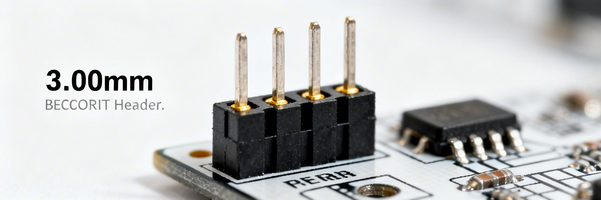
Key datasheet callouts to watch
- ✔ Pitch, pin count, and mechanical keying (polarizing peg).
- ✔ Contact plating material and thickness — affects solderability and long-term resistance.
- ✔ Current rating and rated voltage — drive trace width and clearance.
- ✔ Mechanical life (mating cycles) and operating temperature range.
- Recommendation: Place a one-line spec summary table at the top of any design review doc.
Datasheet at a Glance: Electrical & Mechanical Data
Electrical specs to extract and explain
Use contact resistance to set in-circuit loss budgets; for example, a 10 mΩ contact at 2 A drops 20 mV and dissipates 40 mW per contact — small but cumulative across multiple contacts. Derating at elevated temperature requires larger copper area or parallel conductors for power traces.
| Example Calculation | Result |
|---|---|
| Assumed Current | 2 A |
| Voltage Drop | 20 mV |
| Power Loss | 0.04 W |
PCB Footprint & Layout Requirements
Recommended footprint elements
Create a footprint that includes the recommended drill, an annular ring sized to your PCB fab tolerances, a solder fillet zone on the top side, and a keepout region beneath any polarizing peg to avoid solder wicking. Include a labeled footprint diagram plus a table of drill/pad values pulled verbatim from the datasheet.
Placement & Routing
Route power traces to the header using wide copper pours or multiple vias. Place anchor vias adjacent to the pads for mechanical reinforcement, and consider glue or mechanical anchors for high-mate-cycle applications to reduce solder fatigue.
Assembly, Test & Comparative Insights
Soldering Process
Follow the manufacturer's soldering guidance for wave or selective processes. Ensure solder fillet formation on the tail and validate solderability in pilot runs.
Inspection Criteria
Implement IPC visual inspection criteria for solder fillets. Use go/no-go limits (e.g., contact resistance ≤ specified tolerance × 1.5) before lot release.
Design Scenario
For harness mating in compact devices, add mechanical anchors and ensure the polarizing peg footprint prevents mis-mating.
Final Design Checklist
- ✓ Verify footprint vs. datasheet dimensions (drill, pad, peg).
- ✓ Confirm drill/pad values with PCB fab capabilities.
- ✓ Validate contact resistance on first articles.
- ✓ Run mechanical mating cycle tests for reliability.
- ✓ Confirm environmental margins for enclosure/coating.
- ✓ Traceability: Ensure 43650-0415 part number in BOM.
Summary
- Translate the 43650-0415 datasheet headline numbers into concrete PCB specs.
- Plan for electrical realities: use contact resistance and rated current to set trace width.
- Lock down assembly and test criteria: define soldering process limits and electrical thresholds.





