
RM06F9100CT 0603 910Ω Datasheet: Key Specs & Limits
RM06F9100CT is a 910Ω, 0603 (1.6 × 0.8 mm) thick‑film SMD resistor rated for 100 mW, ±1% tolerance, and a TCR of ~100 ppm/°C, with an operating range of −55°C to +155°C. This datasheet‑focused breakdown gives practical guidance for design decisions: power derating, footprint selection, reflow constraints, and reliability checkpoints to decide when an alternative is required.
(1) At-a-Glance: Core Datasheet Specs (background)
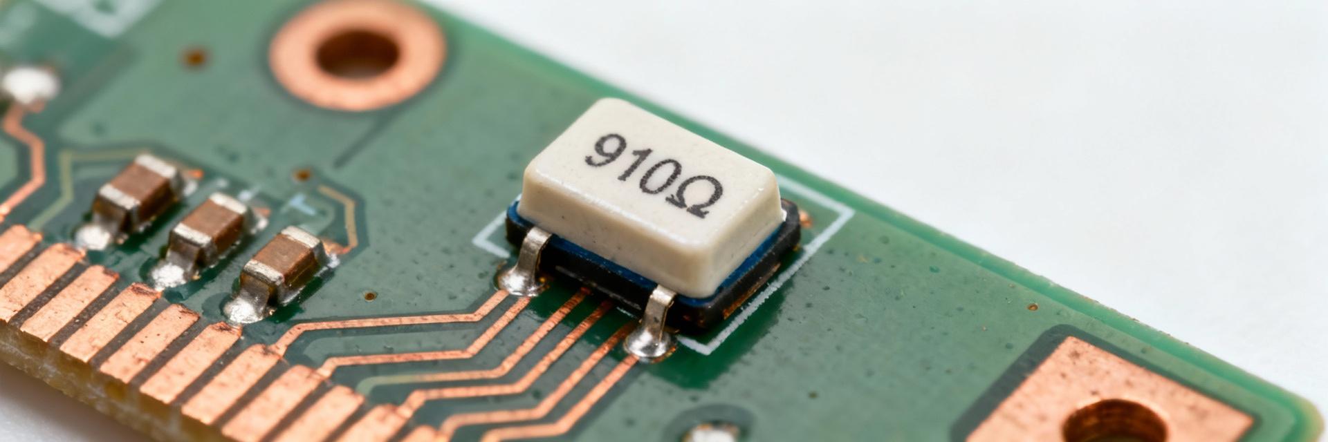
Key electrical specs to list and interpret
Point: Nominal values: 910 Ω, tolerance ±1%, power 100 mW (1/10 W), TCR ≈100 ppm/°C. Evidence: These figures set precision and thermal sensitivity. Explanation: ±1% affects offset in gain stages or reference dividers; 100 ppm/°C means a 0.91% shift over 100°C. Engineers should record these exact values from the datasheet when validating circuits and BOMs; RM06F9100CT should be referenced verbatim when extracting specs.
Mechanical and environmental specs summary
Point: Package and temperature limits matter for layout and reliability. Evidence: 0603 footprint equals 1.6 × 0.8 mm, seated height typically ≤0.55 mm; operating −55°C to +155°C. Explanation: Small form factor limits copper pad area and thermal dissipation; storage handling and high-temperature exposure require verification of solderability and long‑term stability in the target environment. If the datasheet lists a maximum working voltage, use that value for insulation checks.
(2) Electrical Limits & Derating Rules (data analysis)
Power dissipation, ambient vs. board temperature derating
Point: Rated 100 mW is usually valid at 70°C board/reference. Evidence: Real‑world allowed power falls as board temperature rises toward +155°C. Explanation: Use Pd_allowed = P_rated × (T_max − T_board) / (T_max − T_ref), where T_ref = 70°C and T_max = 155°C. Example: at T_board = 70°C, Pd_allowed = 100 mW; at 100°C, Pd_allowed ≈100×(155−100)/(85) ≈64.7 mW. For a 0603 910Ω resistor on a dense board, assume conservative derating and increase copper or move to higher‑power part if board temps exceed ~85°C.
Voltage, noise, and stability constraints
Point: Safe voltage and thermal drift govern use in low‑noise and precision circuits. Evidence: If no max working voltage is listed, calculate V_max = sqrt(P_rated × R). Explanation: For 100 mW and 910 Ω, V_max ≈ sqrt(0.1×910) ≈ 9.5 V. TCR ~100 ppm/°C yields ~0.091% change per °C per resistor, so matched networks or temperature compensation are needed for precision sensing; noise contribution follows typical thick‑film characteristics and should be validated experimentally for sensitive front ends.
(3) Thermal & Reliability Considerations (method / limits)
Thermal impedance and PCB thermal management
Point: Thermal path is resistor → solder → copper → board → air. Evidence: Larger copper pads and thermal vias lower junction‑to‑ambient impedance. Explanation: To increase allowable dissipation, expand copper pour around pads, add thermal relief or multiple vias to inner planes, and avoid isolated small pads. A practical approach is to compare measured board temperatures under load to Pd_allowed and iterate copper area or part choice if the resistor runs hot.
Failure modes, lifetime, and accelerated stress
Point: Common failures are solder fatigue, cracking, and moisture‑related drift. Evidence: Thick‑film 0603 parts are sensitive to cyclic thermal and mechanical stress. Explanation: Request vendor test data: high‑temperature storage, thermal shock, humidity (HAST or 85/85) and solderability. For production, include thermal cycle and vibration on a representative board to catch solder‑fatigue or contact failures before qualification.
(4) PCB Footprint, Soldering & Assembly Guidance (method)
Recommended footprint and stencil notes
Point: Pad geometry and paste coverage affect placement and tombstoning. Evidence: Typical 0603 paste apertures use 60–70% pad coverage per end with split apertures preferred. Explanation: Use symmetric paste openings, avoid excessive paste that creates tombstoning, and tune aperture to ~60% of pad area per side. Follow a conservative reflow profile: controlled ramp, soak where applicable, peak below the resistor’s max soldering limit, and rapid but controlled cooling to reduce stress.
Handling, placement, and inspection checkpoints
Point: Pick‑and‑place parameters and post‑reflow checks prevent assembly defects. Evidence: Use appropriate nozzle, low placement force, and optical inspection. Explanation: Verify resistance after reflow to confirm no open or drift beyond ±1%; inspect fillets for proper wetting and symmetric solder fillets. Acceptance checklist: correct footprint alignment, no tombstoning, measured resistance within tolerance, and no visible cracks.
(5) When to Use RM06F9100CT — Applications & Alternatives (case)
Typical application scenarios
Point: Best suited for low‑power signal and bias networks. Evidence: 100 mW rating and ±1% tolerance fit pull‑ups, pull‑downs, bias networks, and general signal conditioning. Explanation: Use in sensor front‑ends where drift is acceptable within TCR limits, and in digital pull resistors or filtering where small size and common tolerances are adequate.
When to choose alternatives (higher power, lower TCR, tighter tolerance)
Point: Move to alternatives when power, TCR, or tolerance limits are exceeded. Evidence: Triggers: board temp >85°C with heavy dissipation, need TCR
(6) Quick Decision Checklist & Datasheet Extraction Template (action)
8-point design checklist (one-page quick reference)
- Nominal resistance & tolerance verified against circuit error budget.
- Power with derating computed for board temperature.
- TCR acceptable for precision / compensation plan in place.
- Operating temp range covers planned environment.
- Footprint/pad geometry matches assembler recommendations.
- Reflow profile compatible with package limits.
- Reliability tests requested (HTS, thermal shock, humidity).
- If board temp & Pd_allowed conflict, select higher‑power part.
Datasheet extraction template for engineers
- Part number (RM06F9100CT) — record exact string.
- Nominal R, tolerance, TCR, power rating, max working voltage.
- Package dimensions, seated height, recommended footprint and paste %.
- Reflow profile, solderability, moisture sensitivity level.
- Reliability tests and qualification reports to request.
Summary
RM06F9100CT is a 910Ω, 0603 SMD resistor with a 100 mW rating, ±1% tolerance, ~100 ppm/°C TCR, and −55°C to +155°C operating range. Two practical takeaways: (1) apply conservative derating and PCB thermal strategies when operating near the 100 mW limit; (2) verify soldering profile and reliability test data before production. Use the checklist and extraction template to speed design validation and to decide when a higher‑power or lower‑TCR alternative is required. Consult the official datasheet entry in procurement records when finalizing BOMs.
Key Summary
- Power and derating: At board temps above 70°C, compute Pd_allowed with linear derating to +155°C; if Pd_allowed
- Thermal management: Increase copper around pads and add vias to lower thermal impedance and safely raise usable dissipation on the PCB.
- Qualification: Verify solder reflow limits, request thermal shock and humidity tests, and confirm post‑reflow resistance within ±1% before production.
FAQ
What is the maximum voltage across RM06F9100CT?
Answer: If the datasheet does not state a max working voltage, calculate V_max = sqrt(P_rated × R). For 100 mW and 910 Ω, V_max ≈ 9.5 V. Use the vendor‑specified max voltage if provided; otherwise use the calculated value and add safety margin for transients.
How should designers derate a 0603 910Ω resistor on a hot board?
Answer: Use linear derating from the reference temperature (commonly 70°C) to the device max (155°C). Compute Pd_allowed = P_rated × (T_max − T_board)/(T_max − T_ref). If Pd_allowed is insufficient, expand copper, add vias, or select a higher‑power resistor.
What reliability tests should be requested from the datasheet for production?
Answer: Request high‑temperature storage, thermal cycle/shock, humidity (85/85 or HAST), solderability, and mechanical shock/vibration data. Confirm that post‑test resistance drift stays within tolerance and that solder fillet integrity meets assembly acceptance criteria.





