
NL2333ANAE2S-ES: How to Read Electrical Specs & Pinout
Engineers, technicians, and experienced hobbyists often find themselves staring at a datasheet wondering which numbers truly matter for their circuit. This guide offers a practical, step-by-step decode of the NL2333ANAE2S-ES electrical specs and pinout so you can select the right supply, verify performance, and avoid layout pitfalls before committing to a PCB spin. The approach is outcome-focused: extract critical parameters, interpret pin functions and ordering, and apply a concise checklist to integrate the part reliably.
This article emphasizes actionable checks and short verification procedures rather than raw theory. It will show how to spot dangerous absolute limits, how AC and DC figures map to system behavior, and how to read an annotated pinout so you don't rotate a footprint or omit thermal connections. Expect concrete examples, a spec→impact table, an annotated pin diagram, and three bench tests to validate core claims.
1 — Quick Product Snapshot & Why These Specs Matter (background)
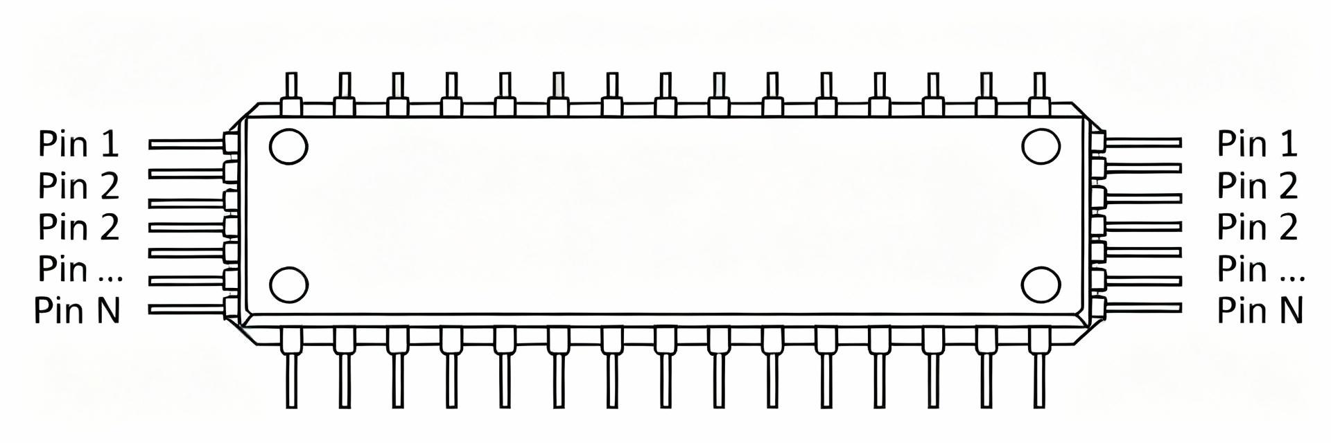
Point: Confirming identity and package details first prevents costly mistakes. Evidence: The full part number, packaging suffix, and channel count define pinout, thermal rating, and ordering accuracy. Explanation: For NL2333ANAE2S-ES, always check full part ID, package type, channel count, and suffix so the board footprint and thermal pad match the shipped device; ordering the wrong suffix can swap pin assignments or reduce temperature range and lead to rework.
1.1 — Key identity points to note
Point: Four to six quick checks reduce supply-chain and layout errors. Evidence: Confirm full part number, package type, channel count, suffix (version/temperature), marking orientation, and tape-and-reel vs tray. Explanation: Mis-ordering a different suffix may change thermal pad size or pin function; wrong package leads to mismatched footprint and electrical failure. Tick these items against the supplier drawing before layout.
1.2 — Which electrical specs directly affect system-level choices
Point: Map datasheet fields to system-level design choices. Evidence: Key drivers include supply voltage range, input/output ranges, offset and bias currents, bandwidth and slew rate, and quiescent/power dissipation figures. Explanation: These specs determine regulator selection, ADC front-end design, signal bandwidth, and thermal strategy; use the table below to translate spec to impact for early design decisions.
| Spec | Design impact |
|---|---|
| Supply voltage (Vcc range) | Determines regulator type, margin, and power sequencing |
| Input common‑mode range | Sets allowable sensor/ADC coupling and resistor network bounds |
| Input offset & bias | Affects measurement accuracy and DC calibration needs |
| Bandwidth / slew rate | Limits maximum signal frequency and amplitude without distortion |
| Quiescent & power dissipation | Drives thermal pad, heatsinking, and battery life calculations |
2 — How to Read the Electrical Specs: Parameter-by-Parameter Breakdown (data analysis)
Point: Distinguish absolute maximums from recommended ranges; quantify how DC specs affect system metrics. Evidence: Absolute Maximum Ratings are limits; Recommended Operating Conditions define safe, repeatable performance. Explanation: For supply voltage, stay within the recommended range to avoid degraded lifetime; consider how a small supply current difference scales in battery applications (e.g., a 15 μA quiescent increase multiplies over millions of hours of field operation).
2.1 — DC specs: voltages, currents, offsets, and rails
Point: DC figures dictate accuracy, interfacing, and power budget. Evidence: Read VCC range, input common‑mode limits, input offset voltage and drift, input bias current, output swing limits, and quiescent current. Explanation: For example, a 100 μV input offset into a 1000× gain yields 100 mV error; a 15 μA extra supply current on a 3.3 V battery can reduce runtime by a measurable percentage—use these numbers to set resistor values, ADC ranges, and regulator headroom when interpreting electrical specs.
2.2 — AC specs: bandwidth, slew rate, settling time, noise
Point: AC specs control frequency response and dynamic accuracy. Evidence: Unity‑gain bandwidth, small‑signal bandwidth, slew rate, settling time, and input/output noise floors. Explanation: Use the rule SR ≈ 2π·f·Vpk to check required slew rate; if you need a 100 kHz, 5 Vpp step then SR ≈ 2π·100k·2.5 ≈ 1.57 V/μs. Check settling time against ADC acquisition windows and ensure noise figures meet your SNR target for the chosen front end.
3 — Pinout & Package: Interpreting Pin Numbers, Functions, and Mechanical Notes (method guide)
Point: Read pin diagrams carefully and verify view orientation. Evidence: Pin 1 marker, top vs bottom view, power pins, I/O pins, NC pins, and exposed pad definitions change layout and thermal performance. Explanation: Misinterpreting view can rotate the footprint 180°, placing rails on wrong nets; always compare the datasheet’s top view and pin table to your footprint and BOM.
3.1 — Reading the pin diagram and pin table
Point: Annotate pins by function and connectivity before layout. Evidence: Create an annotated pin table marking VCC, GND, inputs, outputs, NC, and EP (exposed thermal pad). Explanation: Below is a compact annotated pinout that you can copy into your CAD notes—use it to cross-check pin‑1 orientation and ensure power/ground nets align with the thermal pad and decoupling plan.
| Pin | Function | Notes |
|---|---|---|
| 1 | IN_A | Input channel A, tie to source or bias network |
| 2 | OUT_A | Output A, observe output swing limits |
| 3 | VCC | Supply, decouple close to pin |
| 4 | GND / EP | Exposed pad—solder to board for thermal path |
| NC | No connect | Leave floating per datasheet |
3.2 — Package and PCB footprint considerations
Point: Mechanical details determine solderability and thermal dissipation. Evidence: Recommended land pattern, solder mask clearance, and exposed pad dimensions are in the mechanical drawings. Explanation: Ensure the thermal pad is stitched to a ground plane with multiple vias, confirm solder paste percentages, and verify that component rotation matches the top view. Common mistakes include flipped orientation and omitting thermal vias that cause thermal derating.
4 — Practical Tests & Quick Verifications before PCB Spin (method + case)
Point: Run three bench checks to validate core datasheet claims. Evidence: Supply current measurement, input offset/bias measurement, and output swing under load confirm real-world behavior. Explanation: Use a low-noise supply, proper decoupling, and measurement instruments with resolution better than the spec tolerances to verify that parts meet typical and limit values before committing to a larger build.
4.1 — Bench tests to validate core specs
Point: Practical setups and pass/fail criteria for quick verification. Evidence: Test 1—measure quiescent current with DMM (resolution ≤1 μA), Test 2—measure input offset by applying zero input and reading output with known gain, Test 3—apply a load and sweep supply to confirm output swing and thermal stability. Explanation: For each, record typical vs datasheet limit; failure tolerance is often ±20% of typical for pre-production samples, and oscillation or drift indicates layout or decoupling issues.
4.2 — Common pitfalls and troubleshooting
Point: Typical failure modes and quick fixes accelerate debug. Evidence: Oscillation, unexpected offset drift, pin mis-wiring, and thermal derating are common. Explanation: Checklist fixes include verifying pin mapping with continuity, increasing decoupling close to VCC pin, adding series output resistors or compensation networks for stability, and measuring temperature rise with a thermocouple on the package during load tests.
5 — Integration Checklist & Design Tips (action-oriented)
Point: A concise pre-placement checklist prevents integration errors. Evidence: Confirm exact part number, verify power rails and decoupling, check pin orientation, include thermal pad and soldering notes, and validate operating temperature margins. Explanation: Use the checklist items below to coordinate PCB, layout, and firmware teams—ticking each box reduces the chance of a destructive first spin.
5.1 — Pre-placement checklist for designers
Point: Actionable items for immediate use. Evidence: Confirm exact part number (NL2333ANAE2S-ES), verify VCC and GND nets, decoupling (0.1 μF + 10 μF close), thermal vias under EP, silk and courtyard alignment, and pick proper land pattern. Explanation: Share this checklist with procurement and layout to ensure the correct reel and footprint are used and to prevent orientation errors during assembly.
5.2 — Long-tail considerations and testing before production
Point: Environmental and margin testing ensure robustness. Evidence: Run temperature cycling, humidity exposure if relevant, supply tolerance sweeps, and batch sampling for lot variation. Explanation: Aim for burn-in targets (e.g., 24–72 hours under worst-case load) and sample size guidelines (first rev: 10–30 units depending on risk) to catch early reliability issues before mass production.
Summary — 150–180 words
Reading the NL2333ANAE2S-ES datasheet starts with confirming the exact part ID and package, then extracting the electrical specs that map directly to system needs: supply range, input/output ranges, offset/bias, bandwidth, and thermal limits. Interpret pinout diagrams carefully—identify pin 1, exposed pad, and whether the view is top or bottom—then verify the footprint, thermal vias, and solder mask per the mechanical drawing. Before PCB spin, run three quick bench verifications for quiescent current, offset/bias, and output swing under load, and follow a short pre-placement checklist to prevent orientation and thermal mistakes. Use the spec→impact table, annotated pinout, and test procedures in this guide to reduce integration risk and catch mismatches early; these steps shorten debug time and improve first-pass yield.
Key Summary
- Confirm full part number and package before ordering; mismatches change pinout and thermal behavior and cause assembly rework.
- Prioritize supply range, input/output ranges, offset, bandwidth, and quiescent current when mapping specs to system design choices.
- Annotate the pinout and verify view orientation; expose thermal pad properly with vias to meet power dissipation needs.
- Run three bench tests (supply current, offset/bias, output swing) with clear pass/fail criteria before committing to PCB spin.
Frequently Asked Questions
How do I verify the supply current specification?
Measure quiescent current with a precision DMM in series with the supply, using proper decoupling and with the part in its typical application mode. Allow warm-up time, record typical and worst-case values, and compare against datasheet typical and maximum. If readings exceed limits, check decoupling, stray currents from surrounding circuitry, and part orientation.
What is the best way to confirm the pinout on my footprint?
Cross-check the datasheet’s pin table and top/bottom view against the CAD footprint, verify pin‑1 marker on the silkscreen, and perform a continuity check on a populated board to ensure power and ground pins map correctly. If possible, validate with a single-component test board before full assembly.
How should I test bandwidth and slew-rate for signal integrity?
Use a function generator and scope: apply a known amplitude sine or step, measure gain vs frequency to determine bandwidth, and measure edge slope for slew rate. Compare measured SR to the SR requirement (≈2π·f·Vpk) and check settling time against ADC acquisition windows to ensure the part meets dynamic performance in your system.





