
43045-0418 Datasheet Breakdown: Specs, Pinout & Sizes
A professional deep-dive into the 4-position, dual-row SMT header. This guide extracts actionable specifications, mechanical data, and design best practices for power and mixed-signal PCB applications.
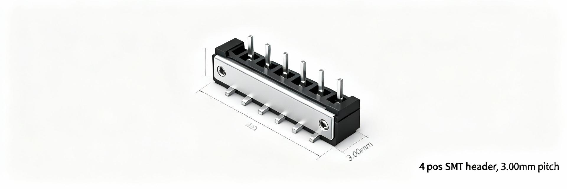
The 43045-0418 datasheet summarizes a 4-position, dual-row surface-mount header with a 3.00 mm (0.118 in) pitch, a typical per-contact current rating around 5 A and a voltage capability up to ~600 V. These numbers determine thermal rise, PCB copper sizing, and insulation clearances; this article extracts the actionable specs, pinout, mechanical sizes, and practical design guidance.
Quick Overview: What the 43045-0418 Is
Role & Common Applications
The 43045-0418 is a dual-row, vertical surface-mount pin header engineered for board-to-board or cable interfaces where modest power and signal distribution coexist. Its 3.00 mm pitch and four-position format make it common for low- to mid-power rails, sensor headers, and I/O breakout connections.
How to Read the Part Code
Part codes typically encode series, position count, and packaging type. Always confirm the mating family and tolerance notes—mismatched packaging or mating family is a frequent source of footprint errors and procurement delays.
At-a-glance Electrical Specs & Limits
*Based on standard thermal rise limits.
*Verify peak dielectric withstand voltage.
| Key Specification | Typical Value / Action |
|---|---|
| Pitch | 3.00 mm (0.118 in) |
| Positions | 4 (dual-row) |
| Current Rating (typ.) | ~5 A per contact — verify in manufacturer datasheet |
| Voltage Capability (typ.) | Up to ~600 V — confirm official value per application |
| Plating | Gold or Tin options — choose based on signal integrity vs. cost |
Pinout, Numbering & Mating Information
Pin Numbering Convention
Establish pin 1 orientation and consistent schematic naming before layout. Typical pinout places pin 1 at a chamfered corner. Map the four positions (e.g., V+, V-, GND, SENSE) and reflect this in silkscreen to avoid mirrored footprint pitfalls.
Mating Interface
Verify mating height and retention geometry. Ensure specified retention force and cycle life meet your application's insertion/removal frequency and vibration environment. Check clearance above the board for cable entry.
Mechanical Dimensions & PCB Footprint
Creating the PCB footprint: Start pad sizes and courtyard with vendor recommendations and add tolerance cushions (+/- 0.1 mm). For the 43045-0418, use the following center-point reference:
| Pad Designation | X Coordinate (mm) | Y Coordinate (mm) | Recommended Shape |
|---|---|---|---|
| Pin A1 | 0.00 | 0.00 | Rect 1.0×0.6 |
| Pin A2 | 3.00 | 0.00 | Rect 1.0×0.6 |
| Pin B1 | 0.00 | 3.00 | Rect 1.0×0.6 |
| Pin B2 | 3.00 | 3.00 | Rect 1.0×0.6 |
Assembly & Soldering
- • Use conservative SMT reflow profiles; verify max peak temperature in the datasheet.
- • Add mechanical solder tabs for power pins to reduce stress on SMT joints.
- • Inspect coplanarity to ensure all 4 pins make reliable contact.
Sourcing & Checklist
- • Check for drop-in equivalents by matching pitch, position, and row spacing.
- • Verify pin-1 orientation matches the board-level assembly drawing.
- • Validate thermal plans with sample testing before volume production.
Summary & Quick Reference
This 4-position, 3.00 mm pitch SMT header is ideal for power/signal interfaces. Always verify electrical limits in the 43045-0418 datasheet.
Apply conservative current derating (~0.7×) when multiple adjacent pins carry heavy loads to manage heat.
Follow footprint guidance, include 3D enclosure checks, and ensure mechanical support for high-stress connectors.





