
1.25mm 9-Pin PCB Header: Complete Datasheet & Pinout
A 1.25mm 9-pin PCB header packs nine signal contacts into roughly 11.25 mm of board space (1.25 mm pitch × 9). This guide provides a datasheet-style breakdown, exact pinout guidance, footprint, and layout tips for US-market hardware engineers and PCB designers.
Quick Overview & Typical Use Cases
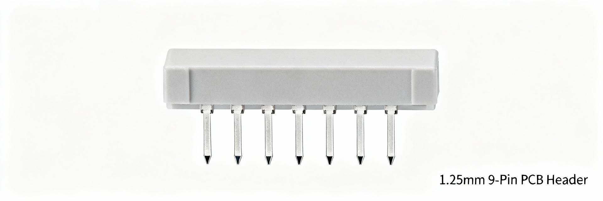
What is a 1.25mm 9-pin header?
A 1.25mm header is a compact single-row connector with 1.25 mm center-to-center spacing; a 9-pin variant contains nine positions. Mechanical families include straight and right-angle, shrouded or unshrouded housings, and through-hole or SMT terminations. In the density hierarchy, it sits between micro wire-to-board pitches and legacy 2.54 mm systems, chosen when board real estate is constrained but logic-level currents are required.
Typical applications in product designs
Common uses include sensor harnesses, internal module interconnects, small display cables, and low-current signal buses. Designers often map I2C, SPI, UART, power, and several GPIOs to a single 9-pin connector for compact modules. The 9-pin PCB header is selected for space savings and sufficient current for logic and small peripherals, enabling compact breakouts and keyed debug ports.
Mechanical & Electrical Specifications
Mechanical Dimensions (Nominal)
*Tolerances typically ±0.05mm for pitch and ±0.1mm for overall length.
Electrical Ratings
| Parameter | Typical Rating |
|---|---|
| Current Rating | ~1.0 A per pin |
| Contact Resistance | 30–50 mΩ |
| Voltage (Withstand) | 100V - 500V AC/DC |
| Plating Material | Tin or Gold Flash |
Pinout & Signal Assignment
| Pin # | Generic Signal (A) | Debug/SWD (B) | Description |
|---|---|---|---|
| 1 | VCC | VCC (3.3V) | Main Power Supply |
| 2 | GND | GND | System Ground |
| 3 | UART_TX | RESET | Transmit / Reset Line |
| 4 | UART_RX | SWDIO / TMS | Receive / Data I/O |
| 5 | I2C_SCL | SWCLK / TCK | Clock Signal |
| 6 | I2C_SDA | SWO / TDO | Data Line / Output |
| 7 | GPIO 1 | TDI | General Purpose / JTAG In |
| 8 | GPIO 2 | UART_TX | Secondary Comm |
| 9 | GPIO 3 | UART_RX | Secondary Comm |
PCB Footprint Best Practices
- ✔ Use rectangular through-hole annuli or oblong SMD pads sized to match plated pin diameter.
- ✔ Specify paste coverage at 60–80% for SMT variants to prevent tombstoning.
- ✔ Reserve keepout space for the mating housing to ensure clearance.
- ✔ Always mark Pin 1 on the silkscreen with a dot or triangle.
Troubleshooting Checklist
Summary & Key Takeaways
Confirm pitch and variant early, document the exact pinout and footprint, and specify plating and current limits to avoid surprises in procurement and assembly.





