RM06F75R0CT 0603 SMD: Complete Specs & Footprint Guide
Design teams choosing compact surface-mount parts need concise, actionable guidance on physical dimensions, electrical limits, and PCB integration. Industry data shows 0603 SMD parts remain one of the most common footprints for passives and LEDs on high-density PCBs because they balance size, manufacturability, and thermal performance. This guide centers on the RM06F75R0CT, outlining what designers must verify in the datasheet and what they should implement on the PCB: physical specs, electrical limits, footprint pads and stencil, reflow profile, and inspection checks.
| Parameter / Dimension | Specification (Metric) | Specification (Imperial) | Engineering Guidance |
|---|---|---|---|
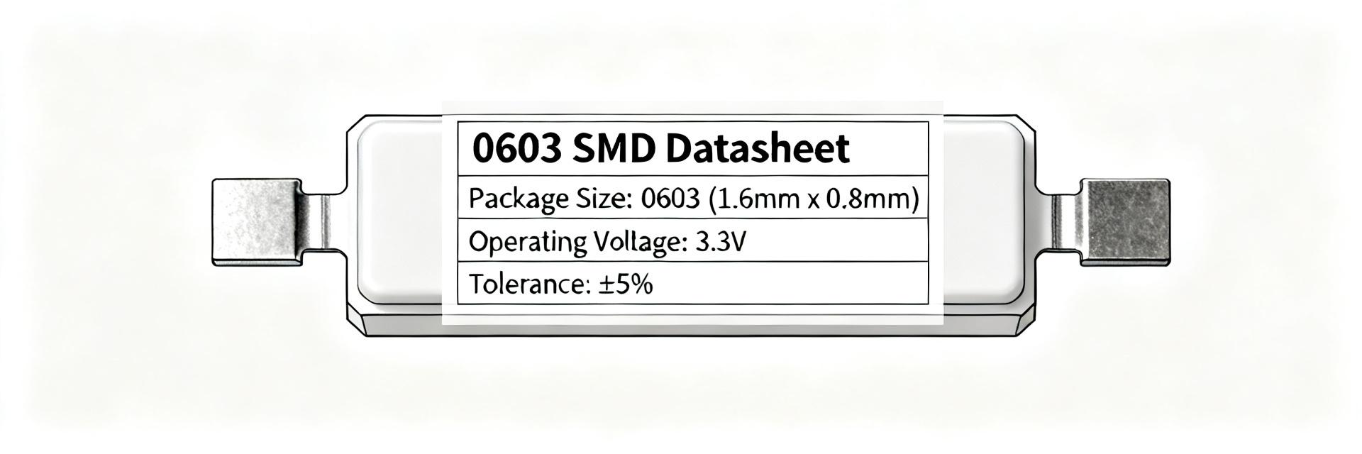
| Component Package Outline | 1.60 × 0.80 mm | 0.063 × 0.031 in (0603) | Standard 1608 Metric footprint profile |
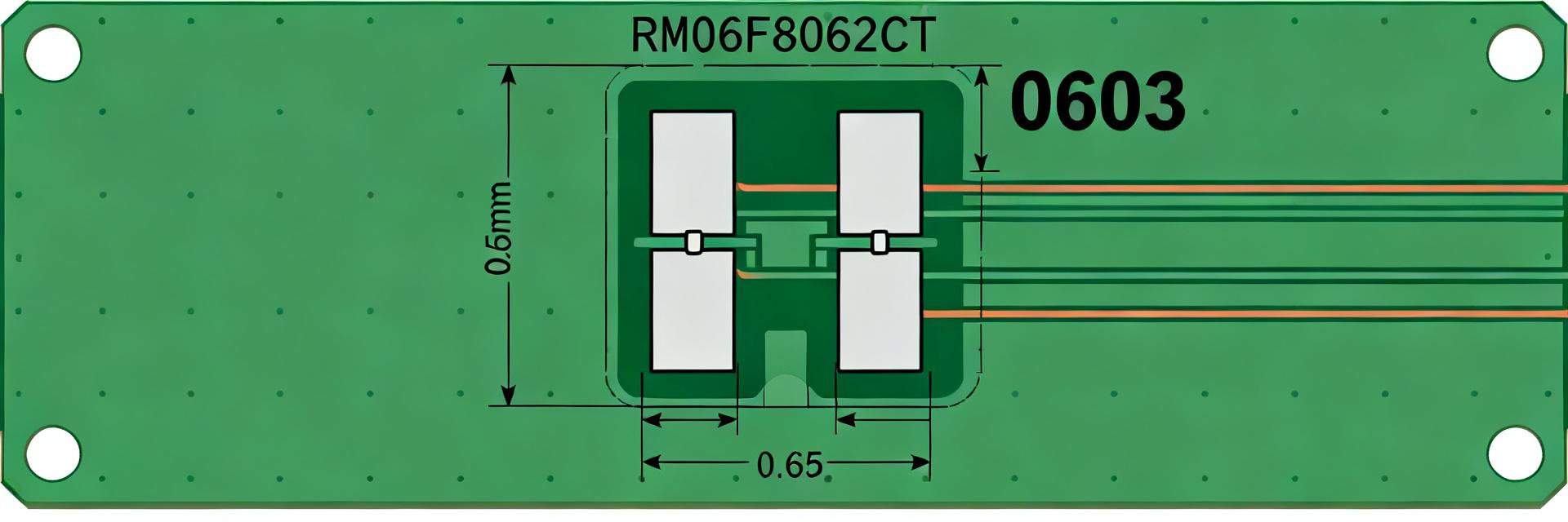
| Recommended Pad Length (X) | 1.30 mm | 51.2 mil | Enables solid solder fillet formation |
| Recommended Pad Width (Y) | 0.60 mm | 23.6 mil | Limits paste excess and prevents lateral bridging |
| Pad-to-Pad Gap (Clearance) | 0.70 mm | 27.6 mil | Centers component body and balances surface tension |
| Target Stencil Thickness | 0.125 mm | 5.0 mil | Laser-cut stainless steel foil |
| Placement Tolerance (X/Y) | ±0.05 mm | ±2.0 mil | Prevents assembly skew and tombstone defects |
1 — Background: What RM06F75R0CT and 0603 SMD mean for your design

Package & physical identity
Point: The 0603 SMD nominal footprint corresponds to a compact rectangular component common for resistors, LEDs, and small passives. Evidence: The canonical imperial size is roughly 0.06" × 0.03" (often represented as 1608 metric or 1.6 × 0.8 mm for LED/resistor variants) with typical thicknesses from ~0.45 mm to 0.9 mm depending on device type. Explanation: For layout and assembly, treat 0603 SMD as a mid-density option—small enough to conserve space, large enough for reliable handling—while confirming the exact device thickness and termination geometry on the part datasheet before defining board stackup or stencil depth.
Typical applications & placement context
Point: 0603 SMD parts are found in indicator arrays, dense sensor boards, and mixed-signal layouts where routing density and reliability must be balanced. Evidence: Compared with 0402, 0603 improves placement robustness and reduces tombstoning risk; versus 0805, it provides better route density at a modest manufacturing cost. Explanation: Choose 0603 SMD when you need a compromise between miniaturization and throughput: place with clearance for reflow fillets, and reserve 0402 for ultra-dense areas or 0805 where mechanical stress tolerance is a priority.
2 — Detailed electrical & environmental specifications (data deep-dive)
Electrical ratings and tolerances
Point: Always extract forward voltage/current, resistance/power rating, tolerance, or capacitance/voltage directly from the RM06F75R0CT datasheet rather than assuming generic 0603 values. Evidence: Datasheets list absolute maximums, typical forward or rated operating points, and tolerance classes; test conditions are commonly stated at Ta = 25°C. Explanation: Use the datasheet tables to set design margins, read derating curves to determine allowable current or power at board temperature, and specify test conditions (Ta = 25°C unless noted) in your verification plan to avoid overstressing the part in application.
Thermal, reliability & lifecycle specs
Point: Thermal characteristics and reliability ratings govern reflow choices and storage handling. Evidence: Key parameters include thermal resistance (θJA), maximum junction and board temperatures, moisture sensitivity level (MSL), and recommended number of reflow cycles. Explanation: Request accelerated test data—thermal shock, humidity soak, solderability—from suppliers when available; set storage and bake procedures based on MSL, and limit rework cycles to preserve device integrity and ensure expected lifecycle performance.
3 — Footprint & PCB land-pattern recommendations (practical footprint guide)
Recommended land pattern dimensions
Point: A PCB land pattern optimized for 0603 parts improves yield and reduces assembly failures; explicitly dimension pads in both mm and mils. Evidence: For a conservative 0603 footprint optimized for the RM06F75R0CT, use pad length 1.30 mm (51 mil), pad width 0.60 mm (24 mil), pad-to-pad clearance 0.70 mm (28 mil), and overall land outline centered on the pads. Explanation: Center the component between pads, define keepout zones equal to the component body outline plus 0.2 mm clearance, and use solder mask between pads to prevent bridging; call this layout the baseline footprint and validate with a mechanical master from the datasheet.
Solder paste stencil and pad aperture tips
Point: Stencil aperture and thickness directly affect wetting and fillet formation. Evidence: For 0603 land pads above, recommend 60–80% paste coverage per pad with a 0.125 mm (5 mil) stainless stencil for balanced paste volume. Explanation: Use 60–80% aperture reduction to prevent excess paste and tombstoning; consider split apertures or windowpanes on longer pads if paste slump is observed. Reference IPC-7351-style clearances when generating Gerber apertures and include an annotated footprint diagram in your release package.
4 — Assembly and reflow soldering best practices
Pick-and-place and placement tolerances
Point: Accurate placement and correct nozzle choice reduce mechanical failures and tombstoning. Evidence: For 0603 components, aim for X/Y placement accuracy better than ±0.05 mm and rotational accuracy within 1 degree; use vacuum nozzles sized for 0603 bodies and program modest pick heights to avoid misfeeds. Explanation: Ensure fiducials and consistent paste deposit volumes to maintain placement repeatability; balance paste volume between pads to avoid tombstoning and confirm stencil cleanliness and flatness for high-throughput lines.
Reflow profile and soldering recommendations
Point: The reflow window must respect device MSL and thermal limits while achieving proper solder wetting. Evidence: Typical reflow guidance for 0603 assemblies: controlled ramp to soak (~1–2°C/s), soak ~60–120s to activate flux, peak 235–250°C for SnPb-free alloys with 30–60s above liquidus, adjusted per MSL and θJA constraints. Explanation: Select solder alloy and flux compatible with the part’s solderability rating, minimize repeated reflows when MSL is high, and watch for assembly warnings—tombstoning, insufficient wetting, or excessive fillet—that indicate stencil, pad, or profile adjustments are needed.
5 — Inspection, testing & troubleshooting on PCB
Visual and X-ray inspection checkpoints
Point: Define clear visual acceptance criteria and X-ray targets for hidden defects. Evidence: Accepted visual checks include continuous fillet on both terminations, coplanarity within component tolerance, no bridging or skew, and no tombstoning. Explanation: Use X-ray to detect voiding under terminations or internal solder defects; common fault signatures include asymmetric fillets (insufficient paste) and internal voids (contaminated paste or poor wetting), which point back to paste aperture or reflow profile issues.
Electrical verification and field troubleshooting
Point: Quick bench tests and a troubleshooting checklist speed failure isolation in production. Evidence: For resistive or LED-type devices, use multimeter continuity and forward-current checks under controlled current; confirm part markings against spec tables before replacement. Explanation: If failures appear, follow a checklist: measure in-circuit continuity, reflow on a toe pad or replaceable test coupon, compare reflow repeatability across boards, and if rework is needed prefer hot-air at controlled temperatures to avoid pad lift; revisit footprint or paste if issues persist.
Summary
- RM06F75R0CT integration requires verifying datasheet electrical limits and thermal specs; ensure board rules reflect derating curves and MSL handling to avoid overstress and premature failure.
- A 0603 SMD footprint with pad dimensions of 1.30 × 0.60 mm and 60–80% paste apertures yields reliable fillets while minimizing tombstoning when paired with a 0.125 mm stencil.
- Controlled reflow profiles, placement accuracy of ±0.05 mm, and targeted visual/X-ray inspection checkpoints form the backbone of a repeatable assembly flow for mid-density PCB designs.
FAQ
How should I verify the RM06F75R0CT electrical ratings before layout?
Check the official datasheet tables for absolute maximums, typical operating values, and test conditions (Ta = 25°C). Cross-reference forward voltage/current or resistance/power entries with your operating temperature and use derating curves to set conservative design margins.
What stencil thickness and aperture percent work best for 0603 SMD parts?
A 0.125 mm (5 mil) stainless stencil with 60–80% aperture coverage per pad is a proven starting point for 0603 parts. Adjust aperture shape (split or windowpane) if you observe excessive solder slump or tombstoning during first-pass assembly trials.
When should I request additional reliability data for a small SMD part?
Request accelerated test data—thermal shock, humidity soak, and solderability—if the part will experience harsh environments, multiple reflow cycles, or long storage. This data helps set MSL handling, bake procedures, and expected field lifetimes.
What are the recommended SMT placement tolerances to prevent tombstoning on 0603 footprints?
Maintain an X/Y pick-and-place alignment within ±0.05 mm and rotational precision within 1 degree. Equalizing paste volume across paired pads and balancing trace thermal relief also significantly prevents imbalance and tombstoning.