RM06F7322CT: Complete 0603 SMD Datasheet Deep Dive
This article extracts the numerical datapoints hardware engineers use most from a typical 0603 SMD datasheet—mechanical dimensions, maximum ratings, thermal resistances, solder/reflow limits, and reliability tests—and shows how those numbers drive footprint, assembly, and validation decisions. The focus is practical: read the datasheet, pick the rows that matter, and act fast.
Intended for PCB designers, hardware engineers, and buyers, the piece gives a numbers-first interpretation so teams can evaluate fit, thermal headroom, assembly constraints, and test requirements quickly. It assumes the reader will consult the component datasheet to quote exact table values during final design and procurement.
Product background & 0603 SMD context
Package & mechanical overview
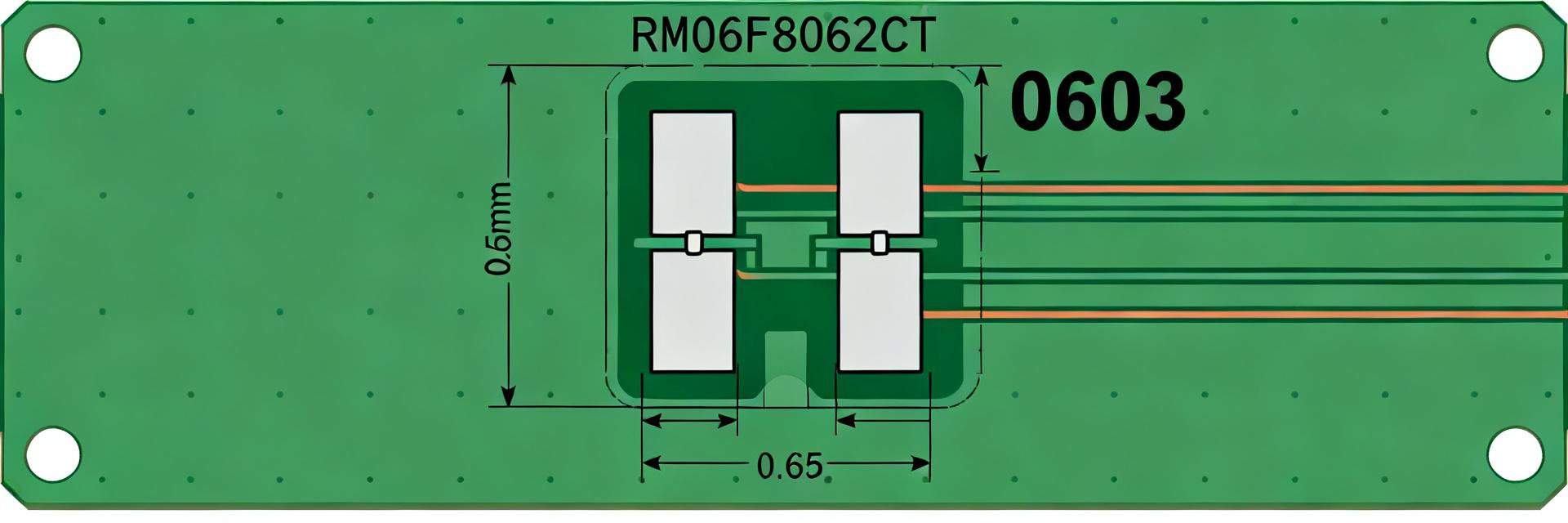
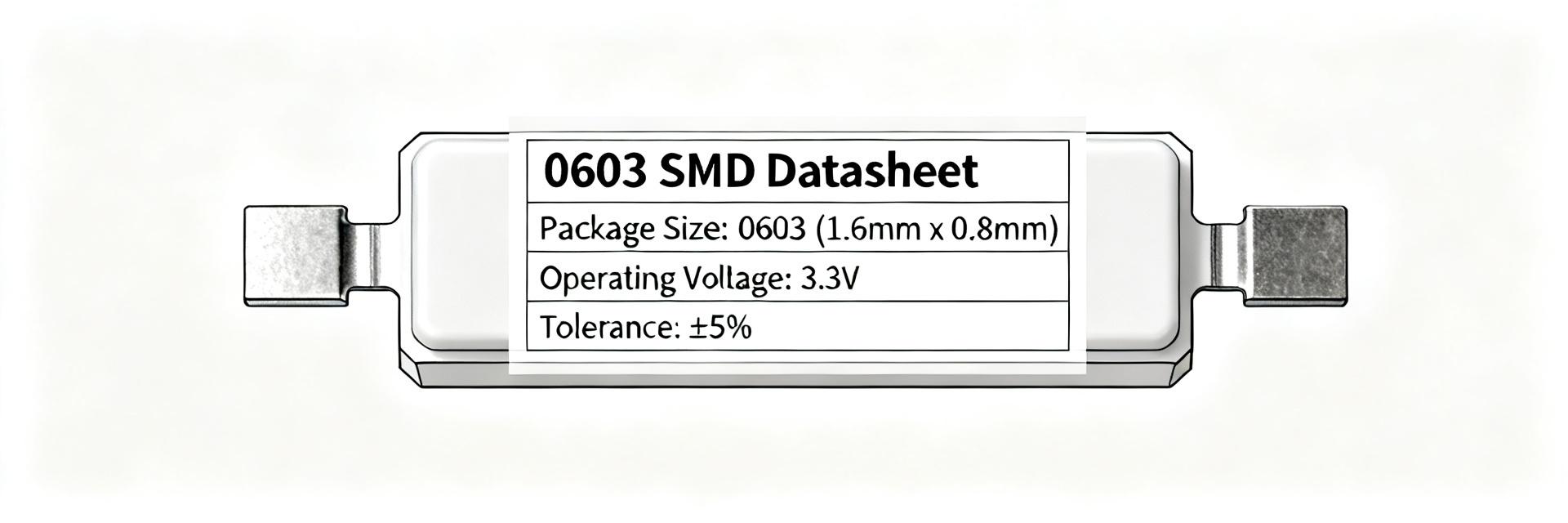
Point: The 0603 SMD nominal footprint is compact and standardized. Evidence: typical 0603 nominal size is 0.06"×0.03" (≈1.6×0.8 mm), with body height varying by series; datasheet mechanical drawings show exact tolerances. Explanation: extract the outline and recommended board pad from the datasheet drawing and use those numbers to generate the footprint and stencil apertures.
Typical applications and where RM06F7322CT fits
Point: 0603 components serve signal-path, indicator, and decoupling roles in dense PCBs. Evidence: datasheet application notes and electrical characteristics indicate recommended uses. Explanation: choose this part when space is constrained and its electrical/thermal limits meet the circuit requirements; otherwise evaluate larger packages for higher dissipation.
Key electrical specifications (data analysis)
| Parameter | Datasheet Baseline | Engineering Rule of Thumb | Design Action |
|---|---|---|---|
| Package Size (EIA/Metric) | 0603 / 1608 Metric | 1.60 ± 0.10 mm × 0.80 ± 0.10 mm | Lock nominal IPC-7351B land pattern |
| Rated Power Dissipation | 1/10 W (0.10 W) at 70°C | Derate by 20% if Ta > 70°C | Calculate P = I²R against thermal ceiling |
| Continuous Working Voltage | 50 V Max (or √P×R) | Apply 20% margin for transient spike | Verify maximum rail voltage limit |
| Resistance & Tolerance | 73.2 kΩ ±1% (E-96) | TC: ±100 ppm/°C typical | Include drift into worst-case loop error |
Absolute maximums and operating ratings to prioritize
Point: Absolute maximum and recommended operating tables are the single most critical reference in a datasheet. Evidence: datasheet absolute‑max rows list voltage, current, and temperature ceilings. Explanation: quote those rows directly into a design checklist, then apply safety margins (typically 10–30%) for production reliability and transient events.
Performance vs. environment: temperature and tolerances
Point: Temperature coefficients and tolerance classes determine worst‑case behavior. Evidence: datasheet tables for tolerance, TC (ppm/°C), and derating curves show how spec limits shift with temperature. Explanation: perform worst‑case calculations (combine tolerance, TC, and ambient swing) to validate margin under highest expected operating conditions.
Thermal behavior & reliability metrics (data analysis / method)
Thermal resistance, junction/ambient temps, and thermal derating
Point: RθJA and RθJC let you convert power dissipation to temperature rise. Evidence: datasheet thermal tables list RθJA (junction‑to‑ambient) and RθJC (junction‑to‑case) values for PCB configurations. Explanation: compute ΔT = P × RθJA for your board, add ambient to estimate junction temperature, and use that to check thermal derating against the datasheet limits.
Reliability testing, lifecycle, and compliance notes
Point: Datasheets list qualification tests and pass/fail criteria that inform production sampling. Evidence: typical entries include high‑temperature storage, thermal shock, vibration, and humidity tests with acceptance criteria. Explanation: map those test types to your product verification plan and require similar samples or certificates from the supplier for qualification.
PCB footprint, assembly and soldering guidelines (method guide)
Recommended footprint & stencil/paste pattern
Point: Pad geometry and solder paste aperture determine placement quality and tombstoning risk for 0603 SMD parts. Evidence: datasheet mechanical drawings include recommended land pattern and tolerances. Explanation: implement the recommended pad size, apply 60–80% paste aperture coverage per pad as a starting point, and include solder mask relief where needed for inspection.
Reflow profile and assembly best practices
Point: The datasheet reflow profile specifies thermal limits and ramp requirements for reliable solder joints. Evidence: reflow tables or graphs give peak temperature and time‑above‑liquidus recommendations. Explanation: follow the component's profile during process development, validate using thermocouples on a representative board, and document handling/ESD precautions for operators.
Comparative analysis & selection guidance (case study / data-driven comparison)
Side-by-side spec checklist (what to compare)
Point: A compact spec checklist simplifies vendor or part comparison. Evidence: compare footprint, max voltage/current, power dissipation, RθJA, tolerance, operating temp, and reliability test matrix from each datasheet. Explanation: capture those rows in a single spreadsheet so you can quickly filter candidates by the constraints that matter most to your design.
Trade-offs and decision matrix for engineers
Point: Selection is a trade-off among size, thermal headroom, and reliability. Evidence: datasheet values for dissipation and test results reveal where trade-offs lie. Explanation: prioritize thermal performance when ambient or power are high, choose smaller packages for space‑constrained low‑power designs, and document cost vs. reliability impacts for the BOM decision.
Practical testing, validation & pre-production checklist (action advice)
Pre-production validation checklist
Point: A short measurable checklist prevents late surprises. Evidence: use datasheet rows to inform each check—footprint match, solderability, max ratings, and reflow profile. Explanation: perform pad-verify (mechanical), pick‑and‑place trial, thermal imaging under rated load, solderability test, and at‑least-one sample reliability run before sign‑off.
Field testing and long-term monitoring recommendations
Point: Field data confirms design assumptions and drives EOL decisions. Evidence: monitor temperature, current, and voltage relative to datasheet limits during burn‑in and pilot builds. Explanation: define telemetry thresholds for drift or excursions that trigger ECOs or replacement, and plan periodic reliability sampling for long‑running products.
Summary
Top datapoints to extract from the component datasheet are: the mechanical footprint (land pattern and tolerances), the primary electrical limit that constrains your circuit (absolute max or operating current/voltage), and the thermal constraint (RθJA and allowed junction temperature). Validate footprint, run thermal checks, and follow the supplied reflow guidance.
Key summary
- Mechanical: confirm 0603 SMD land pattern and tolerances from the datasheet drawing before CAD sign‑off to avoid mis‑placement and rework.
- Electrical: extract absolute maximum rows and operating ratings, then apply safety margins to protect against transients and manufacturing variation.
- Thermal & assembly: compute ΔT using RθJA from the datasheet, validate with thermal imaging, and follow the specified reflow/profile recommendations during process qualification.
Common questions and answers
What are the critical mechanical dimensions for RM06F7322CT?
Check the datasheet mechanical drawing for overall length, width, height, and recommended land pattern. Verify pad-to-pad spacing and tolerances against your PCB CAD rules. Run a pick‑and‑place test with the exact footprint to confirm orientation and placement reliability before volume production.
How do I interpret the absolute maximums in the RM06F7322CT datasheet?
Read the absolute maximum table as non‑operating ceilings; do not use them as continuous operating values. Derive your operating limit by applying a margin (commonly 10–30%) below those values, and validate with worst‑case simulations and sample testing to ensure reliability under transients and temperature extremes.
What thermal data should I extract from the RM06F7322CT datasheet for PCB design?
Pull RθJA/RθJC and any provided derating curves; use ΔT = P×RθJA to estimate junction temperature given your expected power dissipation. Confirm results with board‑level thermal measurements and ensure the design keeps the junction below the datasheet’s allowable temperature across worst‑case ambient conditions.
How do you mitigate tombstoning and assembly defects for 0603 SMD components?
Control pad geometry symmetry, keep paste aperture coverage within 60-80% per terminal, ensure balanced thermal copper distribution across traces, and adhere strictly to the reflow soak profile to guarantee simultaneous solder liquefaction.