
PN 48408-0003 Technical Datasheet: Complete Specs Overview
Technical Snapshot
Point: PN 48408-0003 is a single‑port Type‑A receptacle designed for SuperSpeed USB applications with a 9‑position contact array, typical rated current ~1.5 A per power contact, rated voltage ~30 VDC, operating range −40°C to +85°C, and lead‑free reflow tolerance to a 260°C peak. Evidence: These values are drawn from the component's technical datasheet and mechanical drawing file 484080003_sd.pdf. Explanation: This concise numeric snapshot helps an engineer rapidly decide if the part fits basic electrical, thermal, and assembly constraints before deep review.
Design Objectives
Goal: The article is a focused, single‑page walkthrough of the PN 48408-0003 datasheet so designers can assess fit quickly. Evidence: Coverage includes quick specs, electrical and mechanical analysis, thermal/material notes, PCB layout best practices for USB 3.0 connector SuperSpeed pairs, and a procurement/test checklist. Explanation: Read straight through for selection criteria, or jump to the checklist to validate procurement decisions.
At-a-Glance: Quick Specs & Introduction
Product Identification & Function
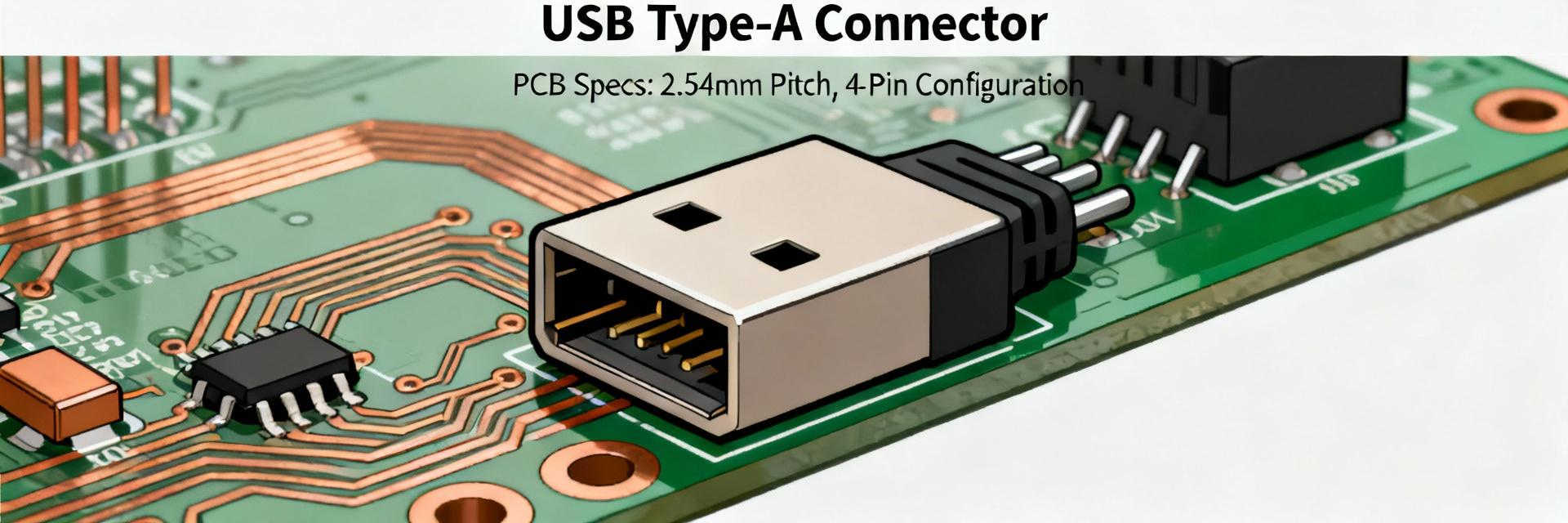
Point: PN 48408-0003 is a vertical, through‑hole Type‑A receptacle intended to provide a board‑mounted USB 3.0 connector interface. Evidence: The part is specified as a 9‑position Type‑A receptacle with through‑hole mounting on its technical sheet. Explanation: That form factor suits PCB edge or bulkhead placements where robust mechanical anchoring is required and simple right‑angle routing is not needed.
Core Numeric Performance Dashboard
Note: These numeric items are the primary selectors for early screening. Match these values against your power budget, enclosure temperature, and assembly profile to determine suitability.
Electrical Specifications Deep Dive
Voltage, Current, and Signal-Level Details
Point: The connector’s electrical limits govern both USB power and SuperSpeed signaling performance. Evidence: The datasheet gives rated voltage (~30 VDC) and rated current per power contact (~1.5 A), and differentiates SuperSpeed differential lanes from USB 2.0 D+/D− pins. Explanation: For power delivery, ensure aggregated current and PCB traces satisfy the per‑contact rating; for signaling, preserve differential pair integrity and avoid loading the SuperSpeed lanes with excessive capacitance or lossy solder joints.
Pinout, Contact Arrangement & Electrical Performance
Point: Pin mapping separates power, USB2 signals, ground, and SuperSpeed pairs into a 9‑contact arrangement; electrical tests establish contact resistance and insulation. Evidence: Typical datasheet values include low contact resistance (<40 mΩ typical) and high insulation resistance, plus characteristic differential impedance control expectations (≈90 Ω). Explanation: Low contact resistance reduces I²R loss on VBUS; designers must reference the exact pin mapping for net assignment and plan TDR or eye‑diagram tests to validate SI across the mated interface.
Mechanical & Dimensional Data
Point: Key dimensions for PCB integration are overall height, board standoff, hole/land pattern, and mating depth. Evidence: The mechanical drawing file (484080003_sd.pdf) contains recommended footprint, hole sizes, and tolerance callouts. Explanation: Use the drawing’s recommended land pattern and tolerance notes to avoid solder fillet interference and preserve mating alignment.
Mounting Note: The part is a through‑hole mounted receptacle designed for wave or selective soldering. Through‑hole anchors carry mechanical loads from insertion; follow fillet recommendations strictly.
Thermal & Materials Reliability
Point: Operating range and reflow tolerance define allowable assembly and ambient conditions. Evidence: Typical operating temperatures are −40°C to +85°C with peak lead‑free reflow around 260°C. Explanation: Confirm your board‑level thermal profile fits the connector limits.
Materials: Housing is high‑temp thermoplastic; contact faces feature gold plating over nickel underplate. Gold reduces fretting corrosion for reliable low‑loss contacts across the ~1,500 cycle lifespan.
PCB Integration & Signal-Integrity Best Practices
SuperSpeed Layout Guidelines
Point: Close to the connector, control differential impedance and minimize discontinuities. Evidence: Datasheet pin positions and mating depth inform where traces exit; SI guidance recommends 90 Ω differential routing. Explanation: Route SuperSpeed pairs as controlled impedance pairs immediately from the connector, avoid T‑stubs, and keep pair lengths matched.
Grounding & Shielding
Point: Proper ground stitching and enclosure connection reduce EMI. Evidence: Mechanical drawing shows anchor pad locations and shield tabs. Explanation: Add ground vias near signal return paths and tie shield tabs to chassis grounds to preserve SI and mechanical integrity.
Application Example & Procurement Checklist
Case Study: Compact Consumer Device
Integration: PN 48408-0003 was integrated into a compact consumer PCB with a shallow plastic enclosure. The vertical through‑hole design provided a low profile and strong board anchoring. Engineers prioritized footprint clearance for mating depth and routed SuperSpeed pairs with 90 Ω impedance to the SoC, achieving clean eye diagrams in validation tests.
📋 Procurement Checklist (5 Essential Items)
- 01 Confirm pin count & orientation against your schematic and PCB footprint.
- 02 Verify rated current/voltage and derate for operating temperature.
- 03 Confirm reflow profile compatibility (peak ≈260°C) and housing UL rating.
- 04 Specify contact plating and RoHS/halogen requirements in the PO.
- 05 Request mechanical drawing PDF (484080003_sd.pdf) and order samples for SI tests.
Executive Summary
- Key Function: PN 48408-0003 is a 9‑position Type‑A, through‑hole USB 3.0 connector offering ~1.5 A per power contact and peak reflow tolerance near 260°C.
- Selection Criteria: Ensure current/voltage ratings meet system power needs, confirm operating temperature range, and verify footprint clearance.
- Next Steps: Obtain the full mechanical PDF, order prototype samples, and perform eye‑diagram and thermal cycling validation.





