
501190-2017 Header Deep Dive: Pitch & Footprint Data
Comprehensive reference for layout, assembly, and procurement decisions for the 501190-2017 dual-row header, focusing on DFM and reliability.
Compact PCBs increasingly demand higher I/O density while minimizing board area, pushing engineers toward fine-pitch, dual-row headers. This deep dive gives a practical, dimension-and-footprint-focused reference for layout, assembly, and procurement decisions for the 501190-2017, emphasizing land pattern, soldering, and DFM considerations for reliable production.
Quick Technical Snapshot
The 501190-2017 is a 20-position, 2-row, vertical SMD header with 1.00mm center-to-center pitch. Constructed with plated contacts over high-temperature polymer, it supports compact board-to-board or cable-to-board interconnects where density and automated assembly are critical.
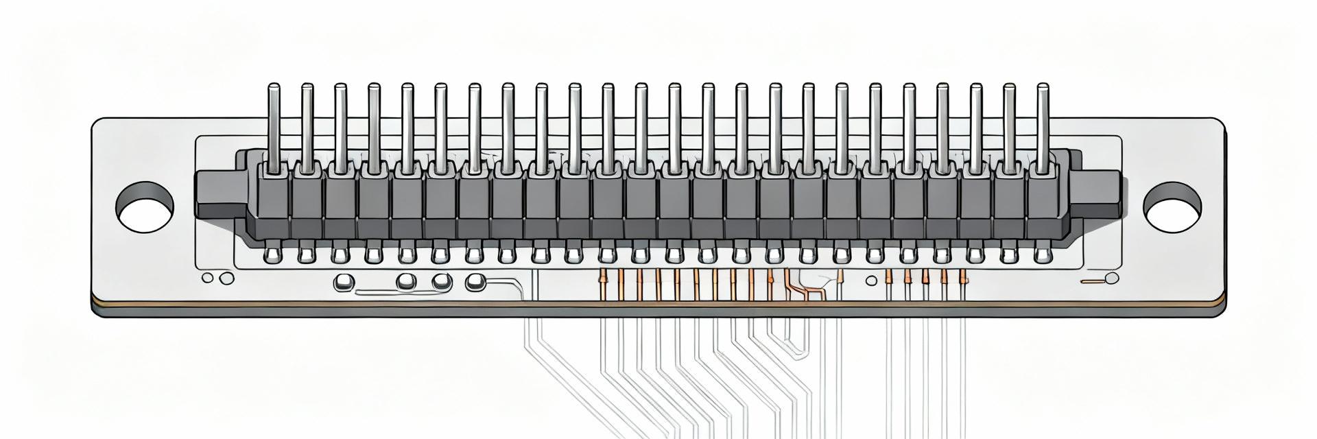
Key Specifications & Procurement Data
| Specification | Typical Value / Engineering Data |
|---|---|
| Positions / Pin Count | 20 (2 Rows × 10 Pins) |
| Pitch (Center-to-Center) | 1.00 mm (0.0394") |
| Orientation | Vertical / Straight |
| Mounting Type | Surface Mount (SMD/SMT) |
| Current Rating (Typ.) |
0.3–1.0 A per pin
|
| Typical Plating | Selective Gold or Tin over Nickel |
Typical Applications
Ideal for dense I/O in small enclosures. Common uses include display module mating, FFC/FPC interposers, compact consumer electronics, and embedded sensor interfaces. The 1.00mm pitch balances density with pick-and-place compatibility.
Pitch Implications
Switching to 1.00mm reduces pad spacing, increasing crosstalk risk and limiting trace clearance. Early layout planning is essential to define microstrip/stripline stackups and maintain signal integrity on 4–6 layer boards.
Technical Deep-Dive: Footprint & Soldering
Signal Integrity & Power
At 1.00mm pitch, impedance control is vital. Maintain trace widths consistent with PCB fab (4–6 mils) and use ground vias for shielding. Route differential pairs on adjacent pins only when required by signal characteristics.
Mechanical Reliability
Expect smaller solder fillets and higher sensitivity to coplanarity. For boards subject to flex or high insertion forces, consider mechanical anchors or board stiffeners. Define keepouts for rework tools early in the CAD phase.
Recommended Land Pattern Geometry
Precise land patterns are crucial for wetting and automated placement. Use elongated rectangular SMD pads with rounded ends.
Design & Assembly Checklist
- ✓ CAD Verification: Run pad-to-pad clearance DRC and verify courtyard outlines.
- ✓ 3D Integration: Fit 3D STEP models into the full-stackup to check interference.
- ✓ Thermal Profile: Use ramp-soak-peak profile (Peak 235–245°C) for SAC alloys.
- ✓ Pick-and-Place: Use local fiducials and ensure nozzle sizes are optimized.
- ✓ Test Strategy: Plan probe/pogo access on the opposite side or via test pads.
- ✓ AOI Setup: Program AOI to inspect fillet presence, coplanarity, and bridging.
Comparative Analysis: 1.00mm Header Density
How the 501190-2017 compares in the design ecosystem:
Practical Recommendations for Procurement
Validate CAD/3D files and assembly behavior prior to volume buys. Request verified land-pattern files, build PCB prototypes with representative solder mask, and run an assembly pilot. Perform mechanical and functional tests to ensure mating connector engagement and electrical continuity before production release.





