47571-0001 microSD 커넥터: 핀아웃 및 데이터시트 깊이 있는 분석
Expert guide for hardware designers on low-profile storage integration.
Designers building compact embedded products rely on low-profile card sockets for removable storage. The 47571-0001 appears in many BOMs because it balances a compact 1.10 mm pitch with an eight-contact layout suitable for SD/SDIO signals. This article decodes the official datasheet, maps the pinout, and gives practical PCB, soldering, and test guidance so you can validate footprint and integration during DFM and DVT.
1.1 Key specs summary (what to list)
Point: Quick spec snapshot helps verify fit and function. Evidence: Datasheet key items include:
| Feature | Specification |
|---|---|
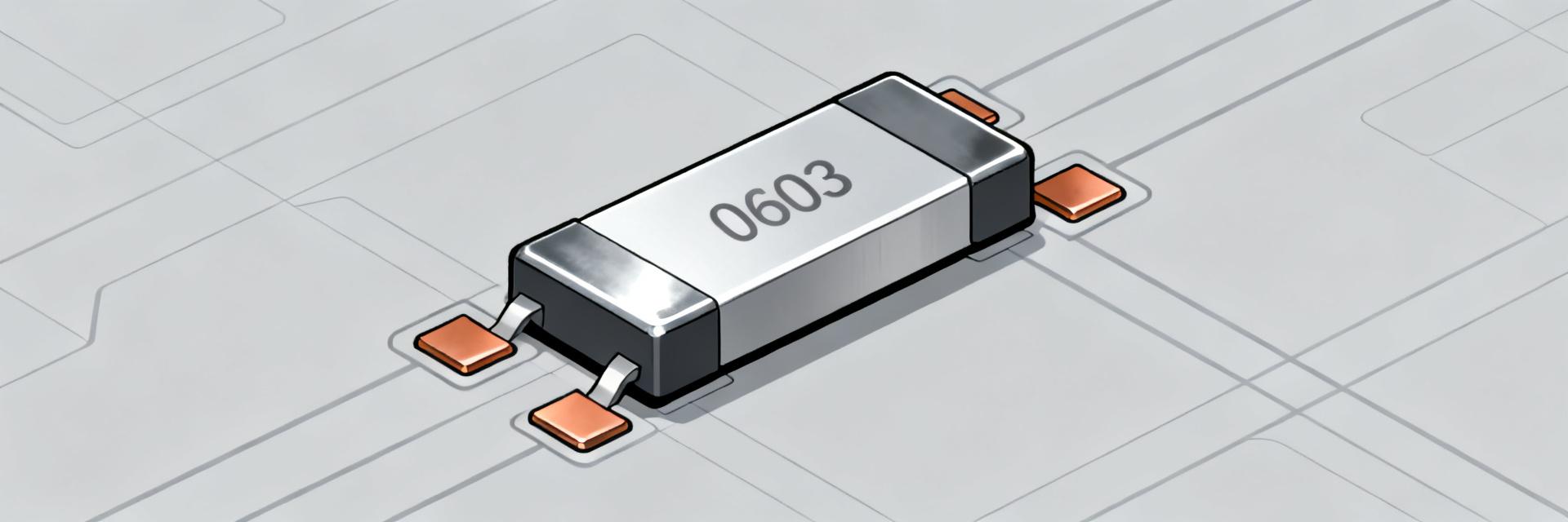
| Pitch | 1.10 mm |
| Contacts | 8-pin Layout |
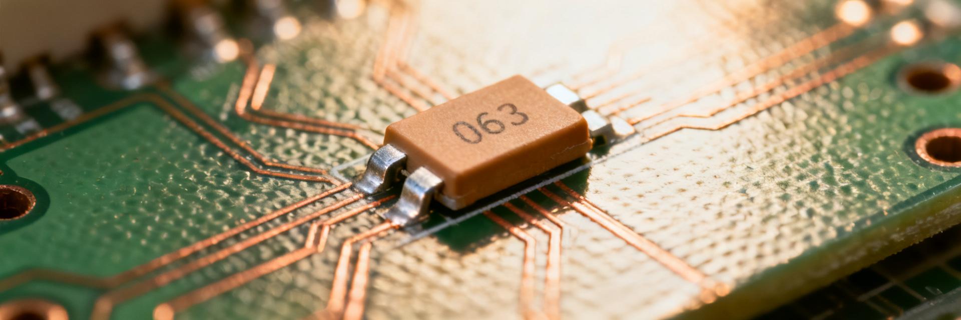
| Termination | SMD (Surface Mount) |
| Switch | Mechanical Card Detect |
| Compliance | RoHS / Lead-Free |
Explanation: Pitch and contact count define routing density; SMD termination and plating affect yield and reliability; the detect switch drives card-present logic and RoHS status impacts process and regulatory compliance.
1.2 Typical use cases & compatibility notes
Point: Typical applications clarify suitability. Evidence: The connector is intended for embedded devices such as cameras, IoT gateways, handheld instruments, and compact consumer electronics per the datasheet usage notes. Explanation: Mechanical form-factor and signal mapping follow microSD electrical/mechanical norms, but you must confirm card insertion force, retention, and the detect-switch polarity against your board logic before committing to a footprint.
Datasheet deep-dive: Mechanical & materials
Point: Mechanical drawings dictate the PCB footprint and keep-out. Evidence: The datasheet provides recommended land patterns, critical dimensions for overall height and insertion depth, and tolerance callouts for solder fillet and coplanarity. Explanation: Use those drawings to define soldermask openings, thermal reliefs, and component keep-outs; incorrect interpretation leads to misalignment, poor solder joints, or insertion interference with nearby components.
2.1 Mechanical drawings & dimensional tolerances
Point: Pay attention to tolerances and assembly notes. Evidence: Typical mechanical views show datum references, critical seating plane heights, and minimum clearance zones. Explanation: Translate these into CAD by locking exact datum points, placing silkscreen-free keep-outs around the card path, and verifying component height relative to any enclosure features to avoid interference during final assembly.
2.2 Materials, plating, and environmental ratings
Point: Contact material and plating affect lifetime and signal quality. Evidence: The datasheet specifies a copper-alloy contact system with gold plating over nickel and a qualifying temperature range and environmental notes. Explanation: Gold plating reduces contact resistance and oxidation risk but enforces specific soldering limits; confirm thermal cycle and vibration specs for product class to ensure reliability under expected environmental stress.
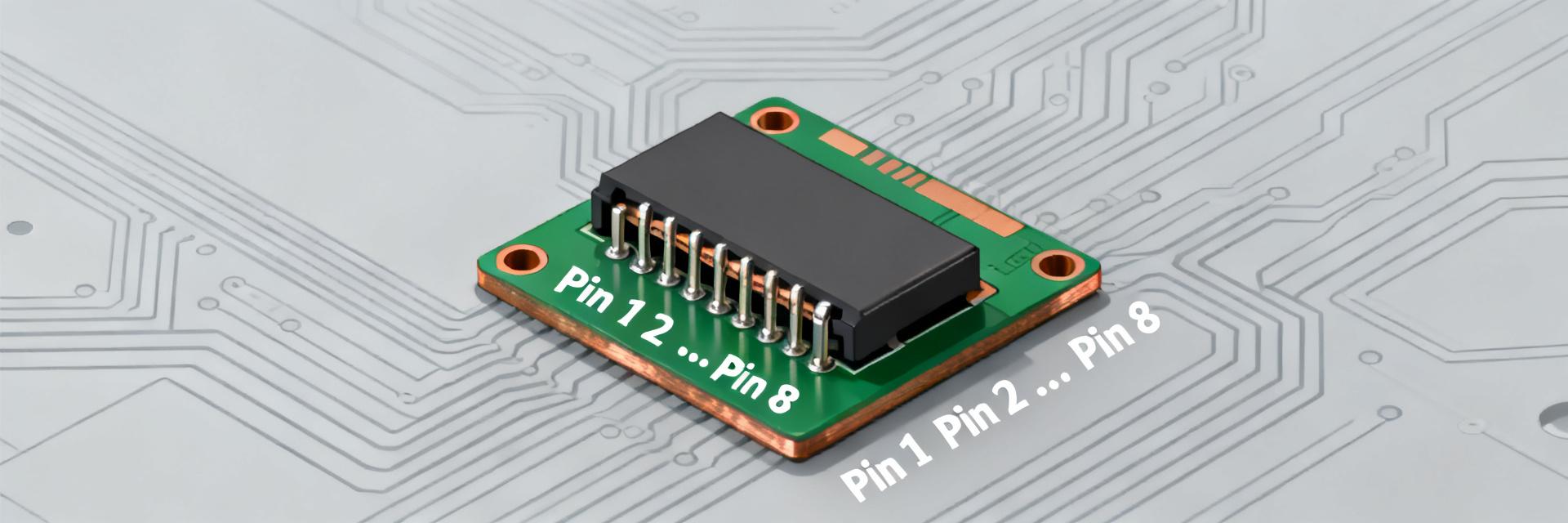
Pinout & electrical characteristics (Data analysis)
Point: Correct pin mapping is essential for routing and card logic. Evidence: The connector maps standard SD signals across eight contacts:
Explanation: Map these pins to your SD host controller with appropriate pull-ups/pull-downs for detect and CMD lines, and keep high-speed signals short and symmetrical to reduce timing skew on 4-bit SD modes.
3.2 Electrical limits & timing notes
Point: Electrical limits inform protection and interface design. Evidence: The datasheet lists contact resistance, insulation resistance, dielectric withstanding voltage, and nominal current ratings for card contacts. Explanation: Use the stated contact resistance and current ratings to size decoupling and protection; implement recommended pull-ups for card detect and follow SD bus timing guidance when moving to high-speed or UHS modes to preserve signal integrity.
PCB footprint, mounting & soldering guidelines
Point: Land pattern translation reduces rework risk. Evidence: The recommended PCB footprint shows pad dimensions, soldermask clearance, and anchor pad placement for SMD pads. Explanation: Use slightly expanded pad-to-stencil ratios for reliable wetting, avoid vias inside primary pad areas, and add soldermask-defined fillets or thermal reliefs to control solder volume during reflow.
4.2 Reflow profile, soldering issues & inspection points
Point: Proper thermal profile and inspection ensure consistent joints. Evidence: The connector is designed for standard lead‑free reflow; the datasheet and common SMD practice define peak temperatures and soak recommendations. Explanation: Watch for defects such as insufficient fillet, tombstoning, or misalignment; include first-piece inspection of solder fillets and coplanarity, and capture X-ray or optical images for high-volume runs.
Real-world integration example (Case study)
Point: A pragmatic layout prevents signal and mechanical problems. Evidence: Best practices suggest placing the connector near the board edge, keeping SD traces short, and using ground pours and decoupling near VDD. Explanation: Route CLK and CMD with controlled impedances where possible, length-match DAT lines for parallel modes, and maintain a solid ground return to reduce EMI and support reliable card operation in noisy environments.
5.2 Validation & troubleshooting test plan
Point: Structured tests catch issues early. Evidence: A recommended test plan includes mechanical insertion cycles, continuity and short checks for each contact, card-detect functional tests, and oscilloscope checks on CLK/CMD for eye shape. Explanation: Define pass/fail criteria (no opens/shorts; detect switch consistency; clean signal edges) and log failure modes to guide design tweaks like pad enlargement or trace rerouting.
Design & Integration Checklist
Point: Pre-procurement checks avoid delivery surprises. Evidence: Verify exact part number, packaging option (tape-and-reel), lead-free/RoHS declarations, and footprint match against your CAD. Explanation: Confirm lifecycle or alternate parts exist to avoid single-source risk, request samples for first-article verification, and ensure documentation includes recommended land pattern and reflow notes.
6.2 Final sign-off items:
- PCB footprint verification in CAD.
- Mechanical clearance test with a physical card.
- Soldering profile validation.
- EMI/ESD mitigations.
- Integration of the DVT test plan.
Key Summary
- 47571-0001 is a low-profile microSD connector with an 8-contact SMD layout; confirm pitch, contact count, and detect-switch polarity from the official datasheet before finalizing the footprint to prevent mechanical or electrical mismatches.
- Mechanical drawings define PCB land patterns and keep-outs; translate datum references, seating plane, and tolerance callouts into CAD rules to avoid assembly interference and poor solder joints.
- Pinout maps DAT0–DAT3, CMD, CLK, VDD, and GND; apply recommended pull-ups for detect logic, route high-speed lines with matched lengths, and validate with oscilloscope checks during DVT.
Common Questions & Answers
How do I verify the connector pinout on my board?
Point: Verification prevents miswires. Evidence: Use a continuity tester or bench multimeter on a mounted sample to confirm each pad maps to the expected signal name per the datasheet. Explanation: Perform this before populating downstream components; confirm detect-switch behavior by inserting and removing a card while monitoring the detect node voltage.
What soldering defects should I watch for with microSD SMD sockets?
Point: Common defects reduce reliability. Evidence: Typical issues include insufficient solder fillet, misalignment, and solder bridging at closely spaced pads. Explanation: Inspect first-piece assemblies optically, measure coplanarity, and adjust stencil aperture or reflow profile to improve wetting and joint formation if defects appear.
Which tests should be included in manufacturing DVT for microSD connectors?
Point: Targeted DVT reduces field failures. Evidence: Include mechanical insertion cycle testing, electrical continuity and insulation checks, card-detect functional testing, and signal integrity spot checks on CLK/CMD. Explanation: Define pass/fail thresholds and retest after environmental stress (thermal cycling/vibration) to validate long-term reliability under intended use conditions.