
52271-1479 Datasheet Deep Dive: 14-Pin 1.0mm Specs
This analysis extracts design-impacting metrics for compact board-to-board and cable-to-board applications, framing the part as a space-efficient FFC/FPC interconnect with technical focus on mechanical, electrical, and signal integrity (SI) verification.
! Practical Design Takeaways
- • Verify PCB footprint drawing callouts to ensure alignment with high-density land patterns.
- • Apply conservative derating rules for current and thermal management.
- • Follow signal-integrity guidelines for the 14-pin array to minimize crosstalk.
Quick Part Overview & Identification
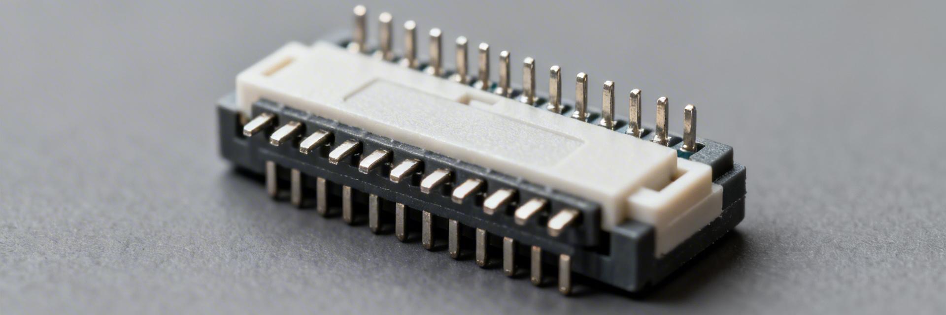
Part Anatomy & Variants
The part identifier encodes series and variant details. The part string typically denotes series, contact count, and orientation. For clarity, always confirm suffixes and ordering codes in the 52271-1479 datasheet to avoid wrong-angle or wrong-contact variants during procurement.
Application Areas
A compact 1.0mm 14-pin connector is targeted at small-signal, low-power links like sensor headers, small displays, and mezzanine connections. Trade-offs favor density over high-current capability; use larger-pitch options for primary power rails.
Mechanical Specifications & PCB Integration
| Parameter | Specification Details |
|---|---|
| Nominal Pitch | 1.0mm (Critical for footprint alignment) |
| Mounting Style | Surface Mount (SMT) / Orientation specific |
| PCB Footprint | Adjust pad expansion & soldermask for assembly yield |
| Reliability | Specified mating cycles and insertion force |
Note: Verify mechanical drawings for row spacing and terminal lengths to prevent tombstoning.
Electrical & Environmental Ratings
Current Capacity (Derating Guide)
Environmental Limits
Temp Range: See datasheet for operating/storage limits.
Durability: Plating type determines high-cycle performance.
Resistance: Factor in insulation and contact resistance for SI.
Signal Integrity & Performance Factors
High-Speed Considerations
Dense 14-pin arrays can introduce impedance discontinuities. Route differential pairs with consistent spacing and isolate sensitive nets. Request vendor SI models for time-domain validation if using high-speed protocols.
Thermal & Stress Management
Contact resistance drives local heating. Use PCB stiffeners and strain relief to prevent solder joint fatigue. Combine contact resistance and expected current to estimate I²R heating during full operation.
Verification & Testing Methodology
Datasheet-to-PCB Checklist
Prototype Acceptance Criteria
Validate continuity/contact resistance before and after mating cycles. Measure insulation resistance and evaluate mating forces. Perform a thermal soak at maximum expected current to confirm safe duty cycles.
Selection, Sourcing & Final Recommendations
Selection Rule
Prioritize 1.0mm pitch for density. If continuous per-pin current exceeds ~0.5 A, consider larger pitch options. Always confirm plating requirements for high-vibration or high-cycle needs.
Risk Mitigation
Lock the exact variant in the BOM. Request sample reels for qualification and verify traceability reports. Maintain version control through the procurement freeze to avoid part substitutions.
Key Summary
- [1] Confirm mechanical drawings and recommended PCB footprints early to avoid assembly yield issues.
- [2] Apply conservative electrical derating; validate with thermal soak tests during prototype phases.
- [3] Address SI and mechanical stress by isolating sensitive nets and utilizing PCB stiffeners.





