TAJA106K006RNJ Fiche technique : Caractéristiques, Tests & Empreinte PCB
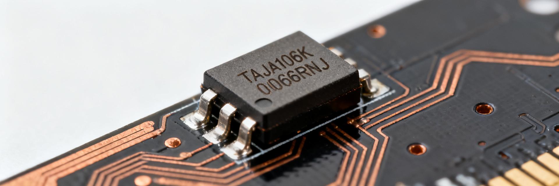
Small solid tantalum SMD capacitors remain central to compact power-rail decoupling because they combine high volumetric capacitance with stable ESR under constrained board area. A typical example is a 10 µF, 6.3 V device in a 3216/1206-class case; these parts are commonly specified where reliable decoupling and low profile are required.
This article delivers a concise breakdown of the TAJA106K006RNJ datasheet, the electrical and reliability tests designers must report, and a verified PCB footprint + assembly checklist that can be applied immediately to a production CAD library and validation plan.
1 — Quick specs & mechanical overview (background)
Key electrical specs to list and format
Point: Extract and present the part’s primary electrical parameters in a compact table for BOM review and validation. Evidence: The official datasheet contains capacitance, rated voltage, tolerance code, ESR, DC leakage, ripple current, impedance vs. frequency and temperature limits. Explanation: Capture each value with test conditions (frequency, temperature) so comparisons and pass/fail criteria are unambiguous.
| Parameter | Value / Notes |
|---|---|
| Capacitance | 10 µF (at 120Hz, 20°C) |
| Rated voltage ($V_R$) | 6.3 VDC up to +85°C (Derated to 4.0 VDC at +125°C) |
| Tolerance | ±10% (K Code) |
| ESR / Impedance | 4.0 Ω Max @ 100 kHz / 20°C |
| DC leakage | 0.6 µA Max (after 5 minutes at rated voltage) |
| Operating temp | -55°C to +125°C (with voltage derating applied above +85°C) |
Mechanical & package data to show
Point: Provide clear mechanical dimensions and polarity orientation for footprint creation. Evidence: The datasheet lists case designation (metric 3216 / imperial 1206-class), recommended length, width, height, polarity marking and the manufacturer land-pattern reference. Explanation: Include exact mm dimensions, marking orientation, and the recommended land-pattern reference ID in CAD notes; always cross-check numbers with the official PDF before release.
2 — Electrical tests & reliability data (data analysis)
Standard electrical tests (how to report)
Point: Define the measurements and pass criteria used on incoming inspection and qualification. Evidence: Typical datasheet test rows specify capacitance test frequency (e.g., 120 Hz), ESR measurement frequency/method (100 kHz), DC leakage voltage and acceptance, and ripple/impulse endurance conditions. Explanation: Report each test with condition table (voltage, temperature, duration), method (LCR meter settings or ESR bridge), and accept/reject limits matched to the datasheet rows for traceability.
Reliability & life test data to interpret
Point: Translate accelerated stress results into usable lifetime guidance. Evidence: Datasheet reliability sections include high-temperature exposure, biased humidity, thermal shock and shelf-life figures plus activation/derating curves. Explanation: Read activation curves to set operating derating (voltage/temperature), estimate expected lifetime under your duty cycle, and convert humidity/thermal results into MTBF-like guides used in power-rail risk assessments.
3 — PCB footprint & land pattern guide (method / practical)
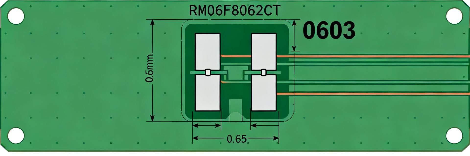
Recommended footprint dimensions & pad layout
Point: Provide a recommended copper pad geometry and tolerances for reliable soldering. Evidence: For 3216/1206-class parts the datasheet recommends an IPC-compatible land pattern and pad clearances; follow the reference pattern and note tolerance bands. Explanation: Example recommended pads (mm, illustrative—verify against datasheet): pad length 1.6 ±0.1, pad width 1.0 ±0.1, pad-to-pad gap 1.6 ±0.1. Final verification in CAD and a STEP model check are required.
Top view (mm, illustrative):
  Pad A (Anode): 1.6 x 1.0   Pad B (Cathode): 1.6 x 1.0
  Center-to-center length: 3.2   End-to-end spacing tolerance ±0.1
  Stencil: 0.125 mm thickness; 60–80% aperture per pad as starting point
Assembly, soldering & reflow considerations
Point: Document reflow and assembly rules to avoid defects. Evidence: Datasheet reflow guidance provides peak temperature windows and recommended profiles for solder paste. Explanation: Use a Med/Lead-free profile with controlled ramp; recommended peak soldering temp per generic practice is within typical reflow windows (verify datasheet), stencil 0.10–0.15 mm, and ensure paste coverage avoids tombstoning — place polarity silkscreen and check post-reflow wetting and fillet formation.
4 — Selection, derating & replacements (method / case)
How to derate and verify suitability by application
Point: Apply practical derating rules for voltage, ripple and temperature to ensure life and reliability. Evidence: For a 6.3 V rated part on a 5 V rail, datasheet derating curves and ripple limits define allowable headroom. Explanation: Use conservative derating: operate below 50% of rated voltage for continuous power rail duty, allow margin for superimposed ripple, and derate temperature per the activation curve; document choices in the part selection rationale.
Finding equivalents and what to match (without vendor names)
Point: When substituting, match the electrical and mechanical criticals. Evidence: Critical parameters to match include capacitance, rated voltage, ESR/impedance at target frequency, temperature rating and case/height. Explanation: Create an equivalence checklist and validate candidate parts in lab (capacitance, ESR, leakage and reflow survivability) before production sign-off.
5 — Practical checklist & validation plan (action / verification)
PCB & BOM checklist before release
Point: Use a concise pre-release checklist that ties footprint and BOM to test artifacts. Evidence: The CAD library entry should reference the datasheet, land-pattern revision and reflow profile. Explanation: Checklist items: footprint verified in CAD and STEP, silkscreen polarity, pick-and-place program validated, datasheet on file, reflow profile validated, storage/packaging handling and supplier quality documentation. Use naming convention like
Post-assembly verification tests
Point: Define the post-assembly validation sequence and instruments. Evidence: Typical checks include in-circuit capacitance, ESR, leakage, visual inspection and thermal cycling; specifications and pass/fail should derive from the datasheet rows. Explanation: Suggested equipment: LCR meter (capacitance 100 Hz–1 MHz), ESR meter or LCR in ESR mode, thermal chamber for +85 to +125 °C cycles, and X-ray for hidden-solder inspection if required; document all results in the build verification report.
Summary
The TAJA106K006RNJ remains a practical choice for compact power decoupling thanks to high volumetric capacitance in a 3216/1206-class case and a datasheet that provides the essential electrical, mechanical and reliability data designers need. Key actions before production are: extract exact numeric rows from the official datasheet, implement the IPC-recommended land pattern in CAD, validate reflow and electrical tests, and enforce a pre-release checklist tied to measured pass/fail criteria.
- Capture the part’s electrical rows (10 µF, 6.3 V, tolerance, ESR, leakage) from the datasheet and store them with the CAD footprint for traceability and test reporting.
- Implement and verify the PCB footprint: follow the datasheet land-pattern reference, use the suggested stencil aperture and perform a STEP-model fit in the CAD library.
- Define electrical tests and reliability acceptance based on datasheet methods (capacitance freq, ESR method, DC leakage and ripple) and record waveforms and limits in the quality folder.
Additional editorial & SEO notes (actionable)
FAQ: Common questions about TAJA106K006RNJ and practical use
What datasheet items are essential to verify for TAJA106K006RNJ before placing on a board?
Verify capacitance with the specified test frequency, rated voltage and tolerance code, ESR/impedance curves at the application frequency, DC leakage at the datasheet-specified voltage and time, maximum operating temperature, and the recommended land-pattern reference. Document each extracted numeric value and the test condition used for measurement.
How should the PCB footprint be named and verified in the CAD library?
Name footprints with the part number plus a revision (for example: TAJA106K006RNJ_FP_v1) and attach the STEP model, the land-pattern reference, and the datasheet PDF. Verify with a physical STEP fit, solder paste aperture simulation, and a first-article reflow run to confirm wetting and placement behavior.
What quick in-production checks catch most soldering or component issues?
Perform post-reflow visual inspection for correct polarity marking and fillet, in-circuit capacitance and ESR spot checks on sample boards, and a leakage test at rated voltage. If anomalies appear, run a thermal cycle and X-ray inspection on suspect boards and record all findings in the failure-analysis log.
What are the recommended voltage derating guidelines for the 6.3V TAJA106K006RNJ in power rail applications?
For standard solid tantalum capacitors like the TAJA106K006RNJ, a minimum voltage derating of 50% is highly recommended for low-impedance circuits (such as power supply input/output filtering). For high-impedance or secondary decoupling lines, a derating of 30% to 40% may be acceptable, but maintaining a safe operating margin below the 6.3V rating ensures long-term reliability and prevents thermal runaway.