تعمق في ورقة بيانات TAJA106K016RNJ — المواصفات وأبعاد التثبيت
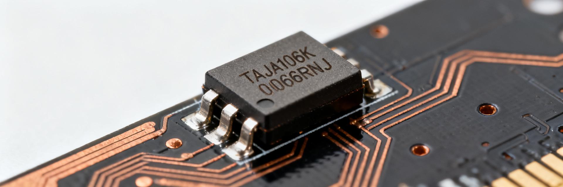
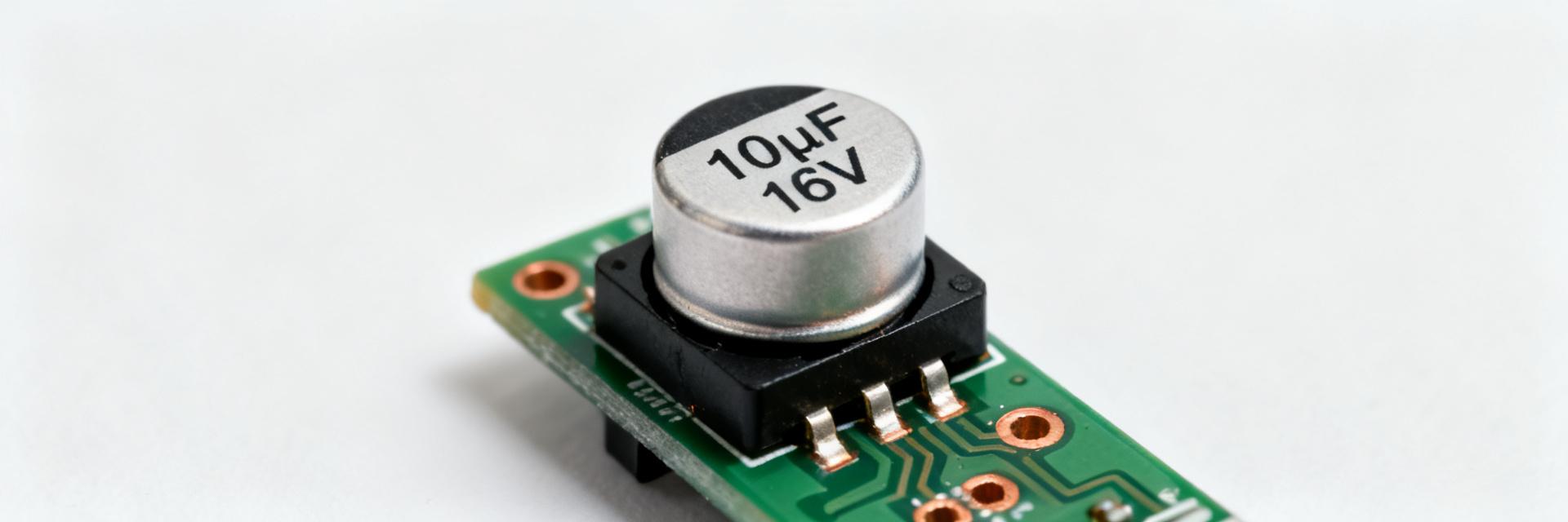
The TAJA106K016RNJ is a high-capacitance molded tantalum SMD capacitor offering 10 µF at 16 V in a 1206 (3216 metric) envelope. This combination of capacitance and compact package makes it a go-to where board area is constrained but energy density and stable ESR are required. A focused datasheet and footprint review reduces layout risk, uncovers thermal and assembly behaviors, and prevents sourcing or assembly surprises for US hardware teams.
1 — Product background: what TAJA106K016RNJ is and typical applications
1.1 — Part family & core role
Point: This part is a molded tantalum SMD capacitor used for decoupling and bulk smoothing. Evidence: Typical use cases include local power-rail decoupling near regulators and smoothing at input stages. Explanation: Designers choose molded tantalum when a stable capacitance under bias and higher ESR than ceramics improve transient damping and inrush management.
1.2 — Package trade-offs and package code meaning
Point: 1206 / 3216 metric denotes ~3.2 × 1.6 mm body; height often ~1.6 mm. Evidence: That footprint yields high volumetric capacitance compared to ceramics in the same planar area. Explanation: Trade-offs include mechanical fragility under flex, a required polarity mark on PCB silkscreen, and careful handling to avoid cracking during placement or reflow.
2 — Datasheet specs deep dive: mechanical & dimensional data
2.1 — Exact package dimensions and footprint-critical tolerances
Point: Core dimensions are 3.2 × 1.6 × 1.6 mm with vendor tolerances on length/width ±0.15 mm typical. Evidence: Datasheet mechanical drawings specify land pattern references and maximum/minimum body outlines. Explanation: Validate your CAD footprint against both recommended land pattern and measured tolerance stack-up to avoid paste starvation or short fillets.
2.2 — Markings, polarity, and mechanical notes
Point: Polarity is indicated by a cathode/anode mark on the part; the datasheet shows recommended silkscreen and polarity keepout. Evidence: Recommended spacing to adjacent pads reduces tombstoning risk during reflow. Explanation: Use clear polarity silkscreen, maintain pad symmetry for correct pick-and-place orientation, and leave modest clearance to accommodate warpage.
3 — Electrical characteristics & performance data
| Parameter | Value / Spec | Notes & Layout Implications |
|---|---|---|
| Capacitance | 10 µF ±10% | Measured at 120Hz; typical DC bias derating applies |
| Rated Voltage ($V_R$) | 16 VDC (85°C) | Derate by 50% for high reliability / transient damping |
| Case Size | A Case (3216 Metric) | EIA Code 1206 footprint equivalent |
| ESR (Max) | 3.0 Ω @ 100 kHz | Provides damping preventing voltage ring in rails |
| Leakage Current ($I_L$) | 1.6 µA Max | Measured after 5 minutes at rated voltage |
3.1 — Capacitance, tolerance, and voltage ratings
Point: Rated at 10 µF ±10% and 16 V. Evidence: Datasheet curves typically show capacitance reduction versus DC bias and temperature. Explanation: Apply derating guidance—expect measurable capacitance drop under DC bias; design margin for low-voltage headroom and ensure capacitance at operating bias meets decoupling needs.
3.2 — ESR, DC leakage, temperature range, and ripple/current handling
Point: ESR is higher than MLCC, leakage and max operating temperature (often up to 125 °C) are given on the datasheet. Evidence: Impedance and ripple current plots identify heating under RMS stress. Explanation: For power designs verify ESR vs frequency for transient damping, sample leakage figures for standby budgets, and confirm ripple current limits to avoid excessive temperature rise.
4 — Footprint & PCB land pattern: designing the pad layout
4.1 — Recommended pad dimensions, solder fillet, and solder mask openings
Point: Pads are larger than ceramic pads relative to body to ensure robust fillet; typical pad lengths ~1.0–1.2 mm. Evidence: Footprint guidance includes solder paste % recommendations (60–80% for end caps). Explanation: Use mid-range paste coverage to balance wetting and fillet formation; too much paste risks tombstoning, too little yields poor fillets and mechanical weakness.
4.2 — Thermal relief, via placement, and creepage/clearance
Point: Avoid via-in-pad directly under end caps unless plated and filled; provide thermal relief when tied to large copper pours. Evidence: Creepage to adjacent copper and mounting stresses are noted in mechanical notes. Explanation: Place vias outside the immediate pad fillet, use ring or dog-bone connections to large pours, and maintain clearance from mounting holes and board edges to reduce stress.
5 — CAD models, footprint verification & real-world examples
5.1 — Where to verify and how to validate footprints in CAD
Point: Validate both 2D footprint and 3D model: overlay mechanical outline, run DRC, and check origin/centering. Evidence: Checklist items should include silkscreen, courtyard, polarity mark, and paste aperture. Explanation: A CAD verification run prevents systematic errors—ensure the 3D solid matches vendor dimensions and the paste % is applied consistently.
5.2 — Example checks from board history (common mistakes)
Point: Two common mistakes: (1) pads too small producing weak fillets; (2) excessive paste causing tombstoning. Evidence: Symptoms include split fillets or lifted components after reflow. Explanation: Remediations are increasing pad land and reducing paste coverage (to ~60–70%) and verifying with a reflow coupon before production.
6 — Layout, placement & assembly best practices
6.1 — Pick-and-place, reflow profile, and handling notes
Point: Use polarity-aware placement, proper fiducials, and reflow profile matched to molded tantalum thermal mass. Evidence: Handling notes include recommendations for placement accuracy and moisture sensitivity controls if specified. Explanation: Verify pick-and-place nozzle programing for small, rectangular parts and include a controlled ramp to peak to avoid mechanical stress.
6.2 — Thermal and mechanical stress mitigation on the board
Point: Place decoupling close to IC power pins and avoid locating caps across flex zones. Evidence: Thermal coupling to large planes increases part temperature during operation. Explanation: Implement thermal reliefs, distribute multiple decoupling caps to spread heating, and keep the capacitor at a distance from screw holes or board edges.
7 — Selection, testing & procurement checklist (actionable)
7.1 — Design-time checklist before finalizing footprint
Point: Confirm dimensions, polarity marking, pad sizes, reflow compatibility, ESR suitability, derating rules, and 3D model fit. Evidence: Cross-check against mechanical drawing and electrical curves in the datasheet. Explanation: Use a design checklist gate to ensure the part will meet both PCB assembly and circuit performance requirements before placing production orders.
7.2 — Incoming inspection and validation tests
Point: Minimum incoming tests: visual polarity check, sample capacitance and leakage measurements, and a reflow test coupon. Evidence: Use thresholds referenced to nominal datasheet values for pass/fail. Explanation: Establish sampling plans and acceptance criteria based on datasheet nominals to catch counterfeit or out-of-spec batches early.
Summary
- Confirm mechanical dims: 3.2 × 1.6 × 1.6 mm and verify vendor tolerances against your CAD footprint to avoid assembly issues; use the datasheet for final verification.
- Electrical suitability: 10 µF, 16 V nominal with expected capacitance reduction under bias; validate ESR and ripple handling for power applications before approval.
- Footprint rules: adopt recommended pad geometry, ~60–80% paste coverage, clear polarity marking, and avoid via-in-pad under end caps to ensure reliable solder fillets.
FAQ
What key datasheet items should I cross-check for TAJA106K016RNJ?
Check mechanical drawing for body and pad recommendations, capacitance vs. bias and temperature curves, ESR/impedance graphs, DC leakage spec, rated temperature, and ripple current limits. These parameters inform footprint, thermal design, and sampling thresholds for incoming inspection.
How do I validate the footprint for TAJA106K016RNJ in CAD?
Download the vendor mechanical drawing and 3D model, overlay over your footprint, run DRC and centroid checks, confirm paste apertures meet % recommendations, and produce a reflow coupon to confirm fillet and tombstone behavior prior to production.
What incoming tests are minimal for production approval?
Perform visual polarity verification, selective capacitance and leakage sampling against datasheet nominals, and a reflow sample test. Use these checks to ensure electrical performance and assembly reliability before approving a lot for full production.
Why is voltage derating critical for the TAJA106K016RNJ?
Molded tantalum capacitors are susceptible to localized dielectric breakdown under high inrush currents. Standard design rules dictate a minimum 50% voltage derating (operating at ≤8 V for a 16 V rated component) to maximize reliability and mitigate transient risks.