1MBI400NA-120-02 IGBT 모듈: 전체 사양 상세 분석
Introduction — Key datasheet figures drive selection decisions. According to the official datasheet, the 1MBI400NA-120-02 is rated for 1200 V blocking and a 400 A collector rating, with a maximum junction temperature in the neighborhood of 150 °C. These headline numbers matter because they set the voltage margin, continuous current capability, and thermal budget engineers must design for when building high-power inverters, motor drives, or industrial converters. This article breaks the datasheet into actionable design guidance so readers can select, size cooling, set gate-drive margins, and run bench validation with confidence.
Scope and outcome: this is a complete spec breakdown and practical design note set. All numerical claims below reference the module datasheet tables and figures; where test conditions matter (Tc, Tj, VGE), those conditions are explicitly stated. After reading, the engineer will know how to interpret static/dynamic tables, estimate switching and steady-state losses, size cooling, and run the key bench tests and troubleshooting checks.
(1) Product overview & quick specs (Background introduction)
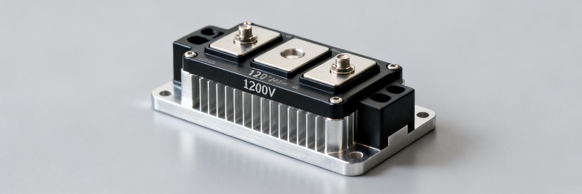
1MBI400NA-120-02 appears on the datasheet as a single high-current IGBT module intended for power-conversion applications. The module format is a bolted baseplate package with multiple power terminals and isolated gate/auxiliary terminals; mechanical drawings in the datasheet show the baseplate outline, terminal spacing, and mounting-hole pattern. Mounting torque and isolation distances are specified in the package drawing and must be followed to avoid mechanical or dielectric failure.
What the part code denotes & package summary
Point: the part code denotes a 1200 V, 400 A single-module class with integrated power terminals. Evidence: the datasheet's mechanical drawing lists the package outline and terminal count and gives explicit mounting-hole diameters and recommended torque for M6 bolts. Explanation: follow the drawing reference and torque spec exactly when installing—over-torque or loose mounting increases thermal contact resistance and risks baseplate distortion; use a calibrated torque wrench and the specified insulating washers where the drawing mandates them.
At-a-glance spec snapshot (electrical, thermal, mechanical)
Point: headline specs to keep top-of-mind are blocking voltage, rated collector current, maximum junction temperature, and thermal resistances. Evidence: datasheet tables list 1200 V Vces(max), 400 A continuous Ic rating, Tj(max) ~150 °C, and Rth(j–c)/Rth(j–s) entries with test conditions (Tc = 25 °C unless otherwise noted). Explanation: present these as a compact spec callout when comparing modules; always note the test conditions shown in the table (e.g., VGE = 15 V for VCE(sat) tests) so design margins are applied consistently.
| Parameter | Typical datasheet value / test condition |
|---|---|
| Vces (max) | 1200 V (table: static limits) |
| Ic (rated) | 400 A (rated, see derating curve) |
| Tj(max) | ~150 °C (junction limit) |
| Package | Bolted baseplate module (see mechanical drawing) |
(2) Electrical characteristics deep-dive (Data analysis)
Static characteristics — VCE(sat), leakage, and DC limits
Point: static tables define guaranteed VCE(sat) at specified VGE and IC, leakage versus VCE and Tj, and DC-rating/derating curves. Evidence: the datasheet provides VCE(sat) values measured at a specified Ic and gate drive (e.g., VGE = 15 V) and leakage Is at stated VCE and Tj points. Explanation: use those conditions to set design margins — for continuous operation pick an operating Ic well below rated Ic according to the module's derating curve (ambient and Tc). For example, limit continuous Ic to the datasheet's recommended percentage when Tc rises above 25 °C.
Dynamic characteristics — switching energies and gate charge
Point: switching tables (Eon, Eoff, Qgs, Qgd) translate directly to switching losses and gate-drive energy. Evidence: the datasheet lists Eon/Eoff measured at specified VCE and IC pulses and gives gate-charge metrics at a specified gate-voltage sweep. Explanation: compute switching loss as Psw = (Eon + Eoff) × f. To estimate Psw for a given switching frequency, take the datasheet energies at the closest test point and scale conservatively, accounting for higher temperatures increasing losses.
Actionable worked example (method): using datasheet Eon+Eoff measured at a representative pulse (state the table and test conditions when applying), Psw = (Eon+Eoff) × f. If the datasheet reports combined switching energy for a specific VCE and IC, multiply by your switching frequency and add conduction loss (Ic^2 × Rds(on)-equivalent or VCE(sat) × Ic duty) to get total device loss for thermal sizing.
(3) Thermal performance, SOA & reliability (Data analysis / methods)
Thermal resistance, junction temperature, and cooling guidance
Point: Rth(j–c) and Rth(j–s) control steady-state dissipation limits; datasheet tables provide these values and Tj(max). Evidence: the datasheet tabulates thermal resistances with clear test condition notes (Tc reference plane). Explanation: compute allowed steady-state dissipation as Pd_max = (Tj_max − Tc_operating) / Rth(j–c). Design with margin (commonly 20–30%) and size heatsinks or liquid cooling accordingly. Prefer a conservative Tc_operating target (e.g., 75 °C) when defining heatsink thermal resistance.
Safe Operating Area (RBSOA, surge capability) and lifetime indicators
Point: RBSOA curves and surge/short-capability figures define transient limits and must be respected. Evidence: the datasheet includes RBSOA plots and short-circuit or surge current specifications with pulse widths and junction-temperature conditions. Explanation: interpret these curves by mapping your expected fault pulse width and amplitude onto the RBSOA plot; include snubbers or current-limiting to avoid operating inside the destructive region. Add reliability tests like thermal cycling and power cycling per datasheet cautions.
(4) Application & design guidelines (Methods / practical)
Gate drive and protection recommendations
Point: correct gate drive amplitude and series resistance control switching speed and robustness. Evidence: datasheet gate voltage limits and recommended VGE are stated in the gate-characteristics table. Explanation: use the datasheet VGE recommendations (e.g., typical +15 V drive, max gate threshold limits) and choose gate resistors to balance switching loss vs. EMI. Implement desaturation detection and a proven short-circuit gate-fail protection circuit for inductive loads.
PCB/mechanical layout, stray inductance and EMI control
Point: mechanical mounting and terminal layout strongly influence stray inductance and dV/dt ringing. Evidence: the mechanical drawing shows terminal placement and recommended busbar practices. Explanation: minimize loop area between C+ and C−, place gate drivers close to module gate pins, and use solid copper busbars or laminated bus to reduce inductance. Verify torque sequence, clean baseplate contact surfaces, and measure contact resistance after assembly.
(5) Testing, sourcing considerations, and troubleshooting (Case & action)
Bench tests to validate datasheet claims
Point: validate key datasheet claims with three bench tests: static VCE(sat) measurement, switching-energy capture, and thermal-rise test at defined Tc. Evidence: datasheet lists test conditions for each measurement; replicate those conditions (VGE, pulse width, Tc) when testing. Explanation: use appropriate current probes, high-bandwidth voltage probes with proper grounding, and a calibrated thermal platform to replicate Tc. Start conservatively on gate drive and limit series inductance during switching tests.
Sourcing, part equivalents, and common fault modes
Point: verify datasheet revision and suffix when sourcing and expect common failure modes like thermal overstress and bond-wire lift. Evidence: the datasheet revision block and part-number suffix information identify critical differences. Explanation: confirm form/fit/functional equivalents by matching package drawing, electrical and thermal ratings, and gate characteristics. Troubleshooting flow: symptom → likely cause → immediate check (e.g., high VCE(sat) → bond degradation → check thermal interface and perform leakage test).
Summary
- Headlines: 1MBI400NA-120-02 is a 1200 V, 400 A class IGBT module with Tj(max) ≈ 150 °C per the official datasheet; use these limits to set voltage and thermal margins.
- Electrical: read static and dynamic tables at their stated test conditions (VGE, Tc) and compute switching losses as Psw = (Eon+Eoff) × f plus conduction losses for total device dissipation.
- Thermal & mechanical: size cooling from Pd_max = (Tj_max − Tc_operating) / Rth(j–c) with 20–30% design margin and follow the package drawing for torque/isolation details.
- Practical checks: implement desaturation protection, minimize stray inductance with tight busbar layouts, and validate with the bench tests outlined above.
- Next steps: consult the official datasheet tables and mechanical drawings for the exact test-condition values before finalizing gate-drive components, heatsink selection, and bench-test parameters.
Frequently asked questions
What gate-drive voltage should I use for the 1MBI400NA-120-02?
Use the gate-drive amplitude specified in the datasheet (typical recommended VGE). Practical practice is a strong positive drive near the datasheet's recommended value (commonly +15 V) and careful selection of gate resistance to balance switching losses and EMI. Always confirm the datasheet gate-voltage limits before finalizing the driver.
How do I estimate thermal dissipation for continuous operation from the datasheet?
Calculate Pd_max = (Tj_max − Tc_operating) / Rth(j–c) using the datasheet Rth(j–c) figure and a conservative Tc_operating. Add a 20–30% safety margin for long-term reliability and account for additional system thermal resistances (heatsink, interface material).
Which datasheet figures are critical when sourcing equivalents for this IGBT module?
Match blocking voltage, rated Ic, package mechanical outline, thermal resistances, and gate characteristics. Verify datasheet revision and suffix to ensure equivalent test conditions and limits; mismatches in package drawing or thermal ratings are common sources of interchange errors.
What is the primary cause of RBSOA violation in this module?
RBSOA (Reverse Bias Safe Operating Area) violations occur when the turn-off voltage spike, driven by stray loop inductance (V = L * di/dt), exceeds the 1200V blocking rating. Minimize stray inductance and use active clamping or snubbers to prevent failure.