54132-4033 FFC/FPC Data Sheet Analysis: Key Specifications & Yields
The 54132-4033 FFC/FPC connector shows how a handful of datasheet entries—0.5 mm pitch, ZIF bottom contact, 40 circuits, contact plating and recommended FFC thickness—drive assembly yield and contact reliability in compact consumer electronics. This article decodes the 54132-4033 FFC/FPC datasheet into concrete design checks, primary yield drivers and a prioritized remediation checklist for production engineers aiming to turn key specs into reliable first-pass assembly.
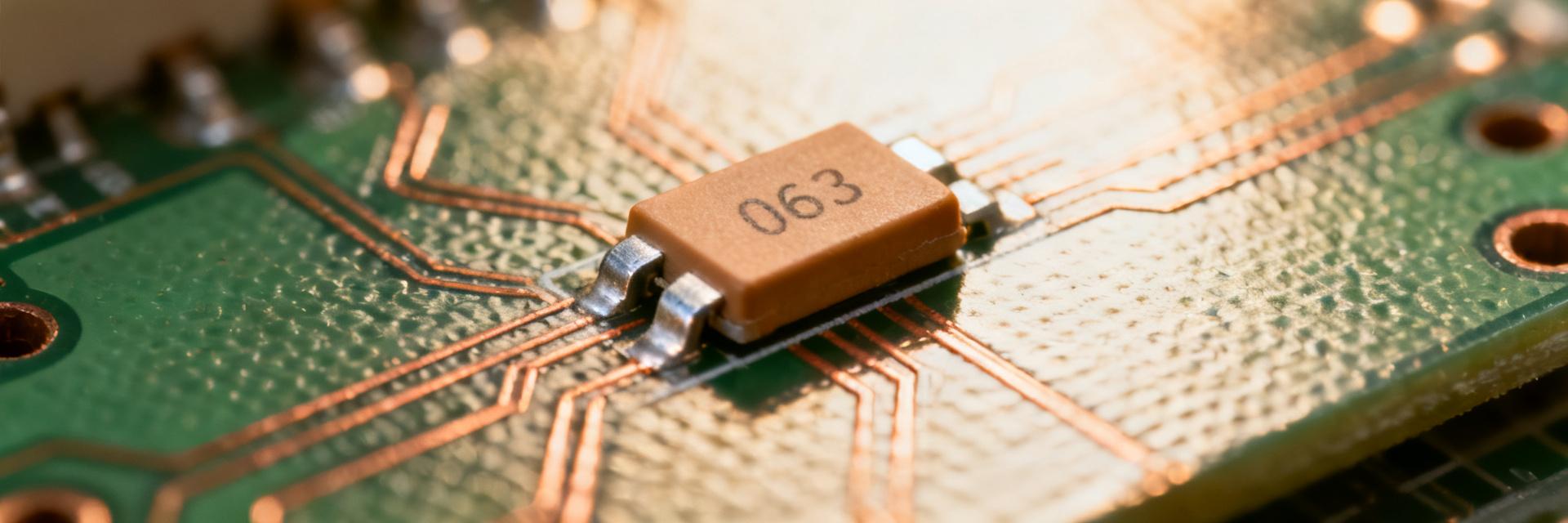
1 Background: What the 54132-4033 FFC/FPC is and where it’s used

Point: The 54132-4033 is a 40-position, 0.5 mm pitch, right‑angle ZIF bottom-contact SMT connector intended for flat flexible cable or printed flexible cable interconnects in space‑constrained electronics.
Evidence: Datasheet callouts highlight pitch, circuit count, contact style, mating height, recommended FFC thickness, current/voltage ratings, plating, and operating temperature ranges as the primary key specs engineers must confirm before layout and process decisions.
Explanation: These specs determine PCB land pattern fidelity, stencil aperture strategy, placement nozzle selection and whether standard reflow profiles and inspection limits are acceptable for the assembly line.
Series summary & key datasheet callouts
Point: Extract headline specs verbatim from the datasheet to avoid misinterpretation during PCB/library transfer.
| Parameter | Datasheet value |
|---|---|
| Pitch | 0.50 mm |
| Circuits | 40 |
| Contact style | ZIF, bottom contact |
| Mounting | Right-angle, SMT |
| Recommended FFC thickness | Refer to datasheet recommended range |
| Contact plating | Tinned finish (per datasheet) |
| Operating temperature | Datasheet specified range |
Evidence: The table condenses the datasheet key specs engineers should paste into the PCB component library. Red flags: (1) plating other than Au on mating surface, (2) narrow FFC thickness window, (3) low mating height limiting solder fillet inspection.
Explanation: Any of these red flags changes test strategy—plating drives lifecycle testing, narrow FFC thickness tightens mechanical tolerances, and low mating height requires AOI/X‑ray workarounds.
Typical applications and constraints in US electronics manufacturing
Point: Typical end-products include compact mobile devices, wearables, small displays and camera modules where board space and low profile dominate design choices.
Evidence: The connector’s 0.5 mm pitch and ZIF bottom-contact style make it a common choice for 0.5mm pitch FFC applications that prioritize minimal height and serviceable cable insertion.
Explanation: Those constraints force stricter stencil designs, tighter placement offset tolerances and targeted inspection (AOI/X‑ray) because misalignment or insufficient solder at 0.5 mm can cause high rework rates.
2 Datasheet deep-dive: electrical, mechanical and material specs (data analysis)
Point: Translate electrical ratings and plating information into test voltages, contact-resistance limits and derating rules used during qualification.
Evidence: The datasheet specifies voltage/current limits and plating type; plating choice (e.g., tin vs. Au) directly affects contact resistance, mating-life and fretting susceptibility.
Explanation: For a tinned contact finish, set acceptance at low single-digit milliohm contact-resistance and plan for lifecycle testing with increasing contact cycles; use dielectric withstand test voltages 2–3x operating voltage per IPC guidance for bench tests.
Electrical ratings and plating/material implications
Point: Convert ratings into actionable test specs: contact resistance, dielectric and insulation tests.
Evidence: Based on the datasheet key specs, recommended test targets include maximum contact resistance (baseline), dielectric withstand voltage and current derating factors consistent with IPC practices.
Explanation: Suggested targets (guideline): contact resistance ≤ 30 mΩ initially, dielectric withstand at 2× rated voltage for 60s as an acceptance test, and current derating margins of 20–30% to account for thermal rise in compact assemblies.
Mechanical and dimensional specs that affect assembly
Point: Tolerances in pitch, pad size and FFC thickness stack and change insertion force and misalignment risk.
Evidence: The datasheet supplies land pattern recommendations and FFC thickness tolerance bands that must be transferred 1:1 to the PCB footprint and DFM checklist.
Explanation: Practice: use the datasheet land pattern, add assembly tolerances (±0.05 mm for pads at 0.5 mm pitch), and verify insertion clearance. Mark retention feature dimensions for jig design and pick‑and‑place collision checks.
3 Yield drivers identified from the datasheet
Point: Identify reflow and contact lifecycle as dominant yield drivers for this part family.
Evidence: 0.5 mm pitch ZIF bottom-contact connectors are sensitive to paste volume, standoff and plating; the datasheet key specs indicate plating and low mating height that affect wetting and fillet formation.
Explanation: Controlling solder-paste aperture fraction and reflow ramp/peak windows is the highest-leverage action to reduce solder-related defects at first pass.
Soldering & reflow-related yield risks
Point: SMT ZIF right‑angle bottom‑contact connectors at 0.5 mm pitch can suffer tombstoning, insufficient wetting and head-in‑pillow defects during reflow.
Evidence: Use a stencil aperture ratio guideline (pad area : aperture area) around 1:1 to 1.2:1 for narrow leads; recommend gentle ramp rates (~1–2°C/s) and controlled peak temperatures compatible with connector materials.
Explanation: Actions: reduce paste volume on small pads (window-pane or segmented apertures), limit soak and peak to the lowest acceptable window to avoid connector warpage, and validate via cross-sectioning and X‑ray for voiding.
Contact reliability & mating-cycle failure modes
Point: Contact force, plating wear and fretting corrosion determine in-field contact failure rates and final-test yields.
Evidence: From the datasheet plating spec and mechanical retention details, define acceptance criteria: contact resistance growth per 1,000 cycles and max allowable change at end-of-life testing.
Explanation: Recommended tests: accelerated mating cycles with periodic contact‑resistance logging, fretting corrosion exposure for mobile/wearable use, and a pass criterion such as ≤50% increase in contact resistance over specified cycles.
Design and process checklist to improve first-pass yield
Point: A compact checklist that translates datasheet land pattern and process limits into pass/fail steps before pilot build.
Evidence: Checklist items come straight from the datasheet key specs and their impact on assembly controls—pad geometry, solder paste type, placement accuracy and reflow curve.
Explanation: Execute the checklist during library signoff and pilot run to minimize rework and reach target FPFY quickly.
PCB footprint, stencil and placement best practices
Evidence & Explanation: Transfer datasheet land pattern exactly, tune stencil apertures, and define placement offsets for the pick-and-place program. Use segmented apertures or 60–80% aperture-to-pad ratio for 0.5 mm pads, select low-tack solder paste optimized for fine-pitch SMT, specify placement offset tolerances ≤ ±0.05 mm and pick nozzle geometry that avoids connector latch damage.
Inspection, test and in-line controls
Point: Define AOI markups and SPC metrics to detect solder and contact issues early.
Evidence: AOI should focus on fillet presence, coplanarity and paste volume; X‑ray is recommended for hidden fillet inspection on low‑profile connectors.
Explanation: Minimal test plan: AOI → electrical continuity/contact resistance → functional FFC insertion test. Track DPM and FPFY; aim to stabilize FPFY within target range (e.g., >95%) across a 2–4 week pilot window.
Troubleshooting & quick-win case actions
Point: Rapid diagnosis paths reduce downtime and restore production yields swiftly.
Evidence: Common symptoms map predictably to causes in datasheet-derived areas: plating, pad design, paste volume, reflow profile, and insertion handling.
Common failure scenarios and root-cause checklist
Symptom → likely cause → immediate test/fix:
- Intermittent contact: Plating wear or debris; test with contact resistance and visual inspection; fix with cleaning or switching to higher-wear plating in next revision.
- Poor wetting: Aperture size or flux compatibility; test with cross-sections and adjust stencil.
Quick wins: low-effort fixes that often raise yields
Point: Implement small process changes with measurable impact during pilot.
Evidence: Typical quick wins include adjusting stencil apertures, changing paste alloy, adding a short pre-bake, or adding a simple insertion jig to standardize FFC mating force.
Explanation: Expected impact: aperture changes (high), paste alloy tweak (medium), pre-bake/clean (low–medium). Validate with KPIs (DPM, FPFY) over 2–4 weeks.
Summary & Next Steps
- Exact land-pattern and stencil strategy for 0.5 mm pitch are primary actions to protect first-pass yield for the 54132-4033 FFC/FPC; confirm pad geometry from the datasheet before library release.
- Design test and lifecycle validation around contact plating and mating cycles—define contact-resistance acceptance and accelerated mating tests informed by the datasheet key specs.
- Implement targeted AOI/functional tests and SPC (DPM, FPFY) early in pilot builds to detect yield gaps and close them quickly.
Frequently Asked Questions
How does the 54132-4033 datasheet affect PCB footprint decisions?
The datasheet provides the authoritative land-pattern and pad-to-pad spacing for the 0.5 mm pitch, 40‑position connector—use it without modification. Deviating pad sizes or spacing increases tombstoning and insufficient-wet issues; retain the datasheet pad and add ±0.05 mm assembly tolerance. Validate with a 5–10 board pilot and inspect paste transfer and post‑reflow fillets.
What are the quickest fixes to improve 0.5 mm FFC solder yield?
Start with stencil aperture tuning (segmented or reduced aperture ratio), switch to a fine‑pitch low-void paste, and tighten placement offset tolerances to ±0.05 mm. These actions typically yield the largest reductions in rework within one pilot cycle when validated by AOI and cross‑section checks.
Which tests should be defined from the datasheet to validate contact reliability?
Define baseline contact resistance, repeated mating-cycle tests (log resistance every defined interval), and fretting-corrosion exposure if applicable. Use an accelerated life plan with acceptance criteria tied to a maximum percent increase in contact resistance over target cycles; record results in SPC for trend analysis.