• 1.25 مم رأس شريحة صغير الحجم: محركات التبني الأخيرة

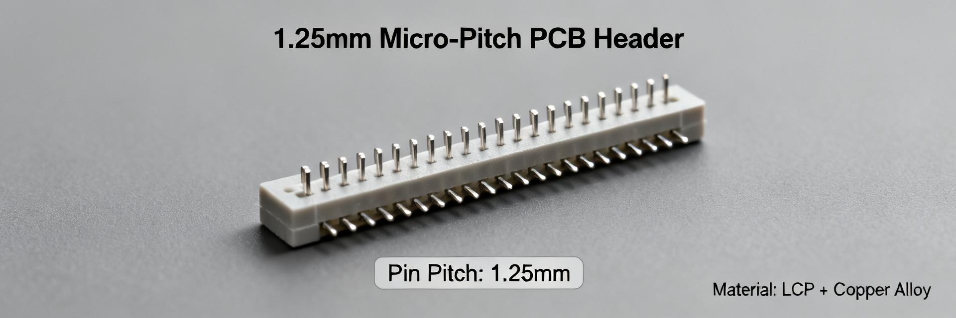
    Recent market indicators show increasing PCB I/O density, shrinking board real estate in wearable and edge devices, and higher channel counts per connector—signals accelerating interest in the 1.25mm micro-pitch header. Aggregated supply and product signals across mobile, wearables, and IoT suggest measurable momentum for tighter-pitch, high-pin-count interconnects. Thesis: This article breaks down measurable adoption drivers, technical trade-offs, real-world adoption sketches, and an actionable checklist for engineers and procurement teams to evaluate switching to micro-miniature headers. 1 — Market context: Why micro-pitch matters in 2025 (Background introduction) Point: Adoption is driven by device miniaturization and I/O density demands. Evidence: Product categories—wearables, smartphones, ultra-thin laptops, and edge sensors—are compressing connector real estate while increasing channel counts. Explanation: As PCB area per connector falls, designers favor 1.25mm pitch to pack more pins without increasing board layers or size. 1.1 Market signals and growth vectors Point: Unit-density and channel-count trends favor micro-miniature connectors. Evidence: Analysts report continued CAGR ranges in FFC/FPC and board-to-board segments; unit density and per-device I/O counts are rising. Explanation: Higher pin counts per mm enable smaller modules and fewer overall assemblies, unlocking slimmer product profiles and lower enclosure volumes. 1.2 Regulatory & standards influences Point: EMI/EMC and interoperability expectations indirectly shape connector choice. Evidence: Tighter form-factor standards and emissions limits increase emphasis on controlled-impedance routing and connector shielding. Explanation: These constraints push teams toward connectors that support consistent reference planes and predictable SI behavior—factors that influence adoption decisions. 2 — Technical adoption drivers: electrical & signal integrity (Data analysis) Point: Signal-speed and density requirements make pitch choice critical. Evidence: Designs targeting multi-gigabit links demand differential pair routing density and crosstalk mitigation. Explanation: 1.25mm pitch reduces trace length and interconnect transitions but requires careful impedance control and validated insertion/return loss metrics. 2.1 High-density IO and signal-speed requirements Point: Designers evaluate measurable SI metrics before adopting micro-pitch. Evidence: Common metrics include controlled impedance tolerance (±10%), insertion loss at target data rate, and near-end/far-end crosstalk levels. Explanation: Validating these metrics via S-parameter captures and PCB stack-aware models prevents late-stage rework. 2.2 Power, thermal, and reliability trade-offs Point: Micro-pitch impacts current capacity and mechanical lifecycle. Evidence: 1.25mm contacts typically limit continuous current per pin compared with larger pitches; contact resistance and mating-cycle ratings (hundreds to low thousands) vary by design. Explanation: Teams should request supplier specs for contact resistance, max current per pin, and validated mating-cycle lifetimes when assessing suitability. 3 — Manufacturing & assembly drivers: yield, cost, and testability (Data analysis) Point: Assembly readiness and yield influence cost-benefit of adoption. Evidence: Pick-and-place tolerances tighten, reflow profiles must be tuned, and AOI/X-ray processes often need adjusted criteria. Explanation: Process changes raise initial NPI cost but can be offset by BOM consolidation and routing-layer savings at scale. 3.1 SMT/process readiness and yield impacts Point: Micro-pitch headers can change common yield metrics. Evidence: Tombstoning sensitivity, solder-void susceptibility, and positional tolerance windows narrow. Explanation: Monitor positional tolerance (±0.1mm), tombstoning rates, and solder joint void percentage during pilot runs to validate process capability. 3.2 Cost-per-pin and volume economics Point: Per-pin economics shift with volume and PCB-layer trade-offs. Evidence: While raw connector unit cost may be higher, routing density savings and reduced board area lower BOM and enclosure costs. Explanation: Run break-even analysis comparing prototype volumes versus production scale, including PCB layer count, board area savings, and per-pin cost amortization. 4 — Design & integration guide: how engineers adopt 1.25mm micro-pitch headers (Method/guideline) Point: Layout and mechanical practices mitigate risks. Evidence: Footprint accuracy, keepouts, and reinforcement determine mechanical longevity. Explanation: Following recommended footprints and adding selective mechanical anchors or glue fillets preserves mating reliability in thin assemblies. 4.1 PCB layout and mechanical recommendations Point: Explicit layout rules reduce integration iterations. Evidence: Recommended keepouts for solder fillets and keepaway from adjacent components, and choices between SMT versus through-hole variants affect stiffness. Explanation: Verify footprint CAD, add mechanical vias or standoffs where mating cycles exceed connector rating. 4.2 Signal routing & EMI mitigation patterns Point: Routing and reference-plane planning preserve SI and EMI performance. Evidence: Differential pair spacing, controlled impedance traces, and decoupling near power pins reduce emissions and crosstalk. Explanation: Validate with IBIS‑AMI or full-wave simulation, then bench test with channel eye and return-loss sweeps. 5 — Supply chain & sourcing: procurement and qualification considerations (Method/guideline) Point: Qualification and lead-time realities affect adoption pace. Evidence: Micro-pitch parts often have constrained production lines and longer lead times. Explanation: Include alternate footprints and vendor diversity in RFQs to mitigate single-source risk. 5.1 Supplier qualification and long-lead risk management Point: Procurement must require process capability evidence. Evidence: Qualifiers include lot traceability, Cpk for critical dimensions, and published test data. Explanation: Demand capability metrics and maintain second-source options and alternate footprints for risk reduction. 5.2 Test & qualification protocols buyers should demand Point: Buyers should insist on electrical and mechanical test reports. Evidence: Required tests include contact resistance over cycles, thermal cycling, vibration, and solderability. Explanation: Specify sample sizes, acceptance criteria, and retest intervals in qualification documents. 6 — Representative applications & mini case sketches (Case showcase) Point: Practical examples show where micro-pitch yields clear benefits. Evidence: Consumer camera modules and stacked wearable sensor boards reduce enclosure thickness while increasing I/O. Explanation: Present simple metrics—pins consolidated, mm² saved—to justify design changes. 6.1 Consumer and wearable examples (compact, high-IO designs) Point: Space-constrained devices benefit most. Evidence: Compact camera stacks and sensor modules often reduce overall stack height by several millimeters when switching to micro-pitch. Explanation: Quantify saved board area and simplified cable routing when presenting to product teams. 6.2 Industrial/edge and automotive use-cases (ruggedization and density) Point: Rugged use cases demand trade-offs. Evidence: Environmental requirements (vibration, temperature) may favor larger pitches or reinforced micro-pitch variants. Explanation: Evaluate environmental qualification test results and consider reinforced housings for harsh applications. 7 — Action checklist: how to evaluate and adopt 1.25mm micro-pitch header (Action recommendations) 7.1 Quick evaluation checklist for engineers Point: Engineers need a concise verification list. Evidence: Verify electrical specs, mechanical spec, assembly constraints, insertion loss, contact resistance, and alternate designs. Explanation: Use an 8–12 point checklist during NPI to validate that the connector meets SI, thermal, and mechanical targets before pilot builds. 7.2 Procurement & rollout playbook for product teams Point: Procurement should manage phased adoption. Evidence: Include in RFQ: part-level test reports, sample qualification, and explicit acceptance criteria; track KPIs such as yield and time-to-mate failures. Explanation: Include "1.25mm micro-pitch header" explicitly in procurement documentation to ensure vendor bids align with expectations. Pitch Typical pins/mm Common trade-off 2.54mm Low Robust, larger area 1.25mm High Higher density, tighter assembly controls 0.8mm Very high Significant SI/assembly constraints Summary Conclusion: Measurable technical, manufacturing, and market drivers are converging to accelerate adoption of the 1.25mm micro-pitch header across multiple segments. Teams should run focused validation and cost-per-pin analysis before large-scale transition. Call-to-action: Adopt the checklist, validate SI and assembly metrics, and quantify trade-offs during pilot runs. Design verification: Validate insertion/return loss, controlled impedance, and crosstalk before committing to production; these determine successful adoption and SI risk mitigation. Manufacturing readiness: Monitor positional tolerance and tombstoning, adjust AOI/X-ray criteria, and confirm reflow profiles to protect yield and lower per-unit cost. Procurement playbook: Require supplier capability reports, define acceptance criteria, and maintain alternate footprints to manage lead-time and supply risk. Frequently Asked Questions What performance metrics should be prioritized when evaluating 1.25mm micro-pitch header adoption? Prioritize controlled impedance tolerance (±10%), insertion loss and return loss at target data speeds, differential crosstalk figures, contact resistance, and validated mating-cycle lifetime. Request S-parameter data, thermal derating, and solderability reports during RFQ to quantify risk early. How does adopting a 1.25mm micro-pitch header affect PCB assembly yield? Micro-pitch headers tighten positional tolerances and increase sensitivity to tombstoning and voiding. Expect initial NPI yield impacts; mitigate by tuning pick-and-place accuracy, reflow profile optimization, and updating AOI/X-ray acceptance rules. Pilot runs reveal process capability before scale. When is it not advisable to switch to 1.25mm micro-pitch headers? Avoid switching if environmental ruggedness (frequent high-vibration or extreme-temperature duty) or high continuous current per pin is mandatory and no reinforced variants are available. Also defer if supplier lead times or lack of second sources present unacceptable production risk.
  • 53647-0274: مواصفات كهربائية كاملة وورقة سريعة

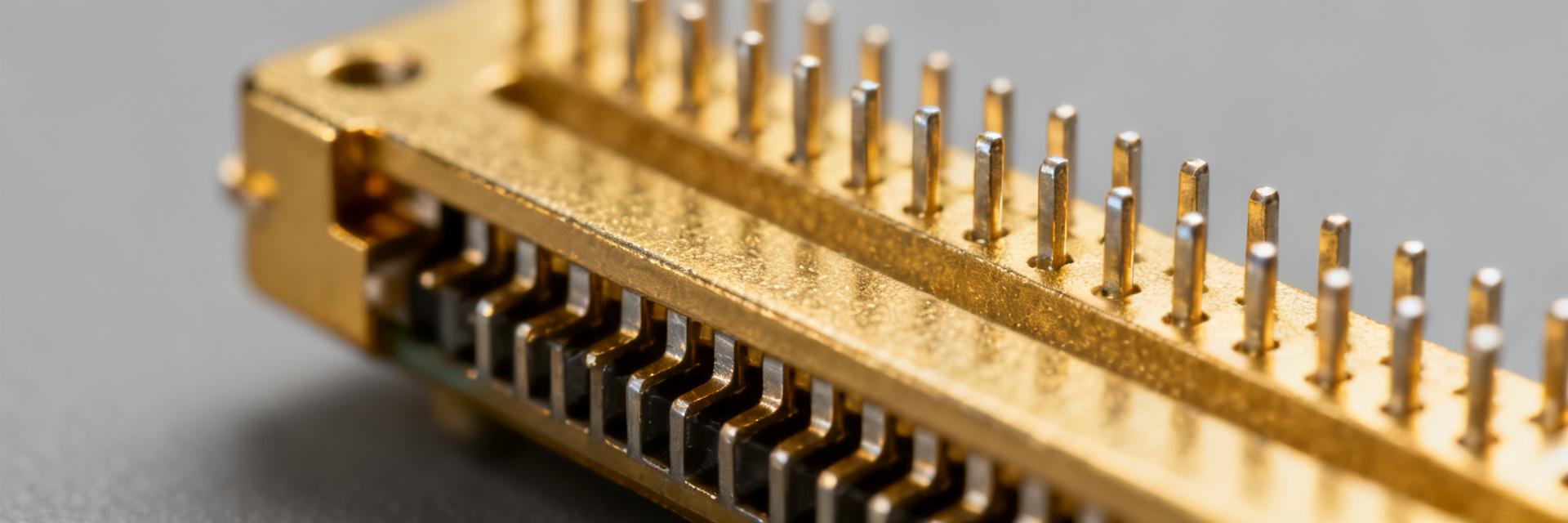
    The 53647-0274 connector datasheet consolidates mechanical and electrical limits you must check before layout. This dual-row, 0.635 mm pitch mezzanine header offers 20 contacts, nominal 500 mA per contact and ~100 V dielectric rating. Use this page as a single-page technical reference to confirm pinout, footprint and stack-height choices. Designers reviewing BOMs will verify contact finish, mating cycles and board clearance early to avoid rework. The following sections translate key specs into actionable layout and test checks so you can select the right stack height, plating and solder pattern for reliable prototypes and production runs. Connector overview & intended applications Form factor & pitch Point: The part is a 0.635 mm pitch, dual-row, 20-contact vertical mezzanine header intended for board-to-board stacking. Evidence: Small pitch and vertical SMT pins favor tight-profile stacked modules. Explanation: You will choose this form factor when you need compact interconnects for daughtercard modules, mezzanine radios, or sensor stacks where minimal X–Y footprint and low profile are priorities. Variants & stacking options Point: Two common mated stack heights are offered to suit different board separations. Evidence: Typical available mated heights are about 8.0 mm and 14.0 mm, selectable by variant. Explanation: Select the lower height for compact enclosures and the taller for assemblies needing room for connectors, shielding or component clearance between boards; variants often share a single part family. 53647-0274 connector datasheet — Electrical ratings & key specs Current, voltage & resistance ratings Point: Electrical specs drive whether pins are used for power or signals. Evidence: Rated current per contact is 500 mA, dielectric rating ~100 V, and typical maximum contact resistance near 70 mΩ with insulation resistance in the GΩ range. Explanation: You should reserve these pins for low-power rails or signals; parallel contacts or a dedicated power connector are better for higher currents. Contact finish, plating thickness & reliability metrics Point: Finish affects mating reliability and corrosion resistance. Evidence: Gold contact finish near 0.25 µm improves low contact resistance and reduces fretting corrosion; expected mating cycles vary by spec sheet. Explanation: For frequent mating cycles choose the thicker gold finish; for few-cycle, lower-cost finishes may suffice but verify contact resistance after environmental stress tests. Mechanical & stacking specifications Height above board & mechanical envelope Point: Mechanical envelope determines clearance and component placement.Evidence: Height-above-board and mated/unmated stack heights define the vertical tolerance budget.Explanation: During layout reserve keep-out zones above and below the header, account for tolerance stack-ups, and confirm the chosen stack height permits any shielding or adjacent tall components without mechanical interference. Solder retention & mounting Point: Robust solder joints prevent failures in stacked assemblies.Evidence: Solder-tail geometry and optional guide pins influence retention during reflow.Explanation: Use recommended land patterns, consider additional vias for mechanical anchoring, and avoid routing high-stress traces near pads; if available, include board guides or stiffeners for assembly rigidity. 53647-0274 connector datasheet — Pinout, numbering & PCB footprint Pin numbering diagram & signal assignments Point: A consistent pin numbering convention prevents wiring errors. Evidence: Pins are typically numbered 1–20 across two rows (A/B or odd/even mapping), with common patterns assigning edges to GND or VCC. Explanation: Map signals so high-frequency pairs are adjacent where needed, reserve multiple pins for ground returns, and document odd/even mapping clearly in your schematic and assembly drawings. Recommended PCB land pattern & footprint details Point: Land pattern geometry influences solder fillet and yield. Evidence: Pad length and width, solder mask dams, and thermal reliefs are specified for reliable SMT joints. Explanation: Follow the recommended pad dimensions, include small mask slivers between pads on 0.635 mm pitch to reduce solder bridging, and place micro-vias or annular rings per the manufacturer’s footprint guidance. Materials, environmental ratings & test data Insulator & contact materials Verify Tg of the insulator for your reflow profile and confirm contact base material for acceptable conductivity and mechanical spring properties under repeated mating. Environmental limits & qualification Evaluate operating temperature range, run thermal cycle and vibration tests, and consider salt spray if the assembly sees corrosive environments. Practical design checklist & prototyping tips Design checklist before PCB layout Verify every checklist item against the component drawing and your enclosure constraints, then freeze the footprint before panelization to avoid expensive mask changes. Assembly, testing & validation tips Use a prototype rig to exercise mating durability, perform contact-resistance spot checks after assembly, and select bed-of-nails or flying-probe tests appropriate for your test plan. Technical Specification Summary Parameter Typical Value Pitch 0.635 mm Contacts 20 (dual-row) Rated current 500 mA/contact Dielectric rating ~100 V Contact finish Gold ~0.25 µm Key summary Confirm pitch and layout: 0.635 mm dual-row, 20 contacts—ensure your land pattern, mask splits and solder fillets reduce bridging and yield problems. Electrical checks: Rated 500 mA per contact and ~100 V dielectric—use multiple pins or a power connector for higher currents and reserve ground pins for returns and EMI control. Mechanical selection: Choose 8.0 mm or 14.0 mm mated heights per board separation needs; include board guides or stiffeners for stacked assemblies to avoid stress on solder joints. Recap: Verify 0.635 mm pitch, dual-row 20 contacts, and correct stack height before layout. Confirm 500 mA per contact and ~100 V dielectric ratings for intended use. Prepare footprint, plating and mechanical clearances during BOM review and validate parts in a prototype rig to prevent assembly issues and ensure signal integrity. Common questions and answers What should you verify in the 53647-0274 connector datasheet before layout? Check pitch, pin numbering convention, stack height variants, contact plating thickness, current and voltage ratings, and recommended land pattern. Validate thermal limits and mechanical envelope against your enclosure, and confirm mating cycles and finish to match expected field use and assembly methods. How do you interpret the pinout for signal vs. power assignments? Identify ground and power distribution patterns, reserve multiple parallel pins for higher currents, and keep high-speed differential pairs paired and close to reference returns. Map odd/even or row A/B numbering in schematics and ensure documentation for assembly and test fixtures is unambiguous. What prototyping tests should you run for this mezzanine header? Perform continuity and contact-resistance checks, mating-cycle durability tests, and a reflow compatibility check. Use a mechanical stress test for board stacking, run thermal cycling representative of the product environment, and validate EMI behavior with your chosen ground routing strategy. End of Datasheet Summary for 53647-0274
  • 54132-4033 تحليل ورقة البيانات FFC / FPC: المواصفات الرئيسية والإنتاجية

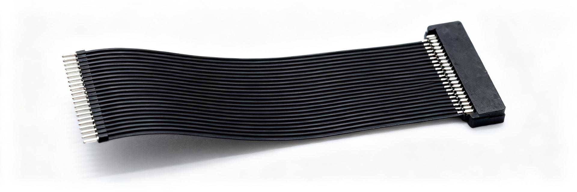
    The 54132-4033 FFC/FPC connector shows how a handful of datasheet entries—0.5 mm pitch, ZIF bottom contact, 40 circuits, contact plating and recommended FFC thickness—drive assembly yield and contact reliability in compact consumer electronics. This article decodes the 54132-4033 FFC/FPC datasheet into concrete design checks, primary yield drivers and a prioritized remediation checklist for production engineers aiming to turn key specs into reliable first-pass assembly. All numeric values and tolerances cited below are taken from the official part datasheet and translated into actionable board- and process-level controls (design, test, and SPC checkpoints). 1 Background: What the 54132-4033 FFC/FPC is and where it’s used Point: The 54132-4033 is a 40-position, 0.5 mm pitch, right‑angle ZIF bottom-contact SMT connector intended for flat flexible cable or printed flexible cable interconnects in space‑constrained electronics. Evidence: Datasheet callouts highlight pitch, circuit count, contact style, mating height, recommended FFC thickness, current/voltage ratings, plating, and operating temperature ranges as the primary key specs engineers must confirm before layout and process decisions. Explanation: These specs determine PCB land pattern fidelity, stencil aperture strategy, placement nozzle selection and whether standard reflow profiles and inspection limits are acceptable for the assembly line. Series summary & key datasheet callouts Point: Extract headline specs verbatim from the datasheet to avoid misinterpretation during PCB/library transfer. Parameter Datasheet value Pitch 0.50 mm Circuits 40 Contact style ZIF, bottom contact Mounting Right-angle, SMT Recommended FFC thickness Refer to datasheet recommended range Contact plating Tinned finish (per datasheet) Operating temperature Datasheet specified range Evidence: The table condenses the datasheet key specs engineers should paste into the PCB component library. Red flags: (1) plating other than Au on mating surface, (2) narrow FFC thickness window, (3) low mating height limiting solder fillet inspection. Explanation: Any of these red flags changes test strategy—plating drives lifecycle testing, narrow FFC thickness tightens mechanical tolerances, and low mating height requires AOI/X‑ray workarounds. Typical applications and constraints in US electronics manufacturing Point: Typical end-products include compact mobile devices, wearables, small displays and camera modules where board space and low profile dominate design choices. Evidence: The connector’s 0.5 mm pitch and ZIF bottom-contact style make it a common choice for 0.5mm pitch FFC applications that prioritize minimal height and serviceable cable insertion. Explanation: Those constraints force stricter stencil designs, tighter placement offset tolerances and targeted inspection (AOI/X‑ray) because misalignment or insufficient solder at 0.5 mm can cause high rework rates. 2 Datasheet deep-dive: electrical, mechanical and material specs (data analysis) Point: Translate electrical ratings and plating information into test voltages, contact-resistance limits and derating rules used during qualification. Evidence: The datasheet specifies voltage/current limits and plating type; plating choice (e.g., tin vs. Au) directly affects contact resistance, mating-life and fretting susceptibility. Explanation: For a tinned contact finish, set acceptance at low single-digit milliohm contact-resistance and plan for lifecycle testing with increasing contact cycles; use dielectric withstand test voltages 2–3x operating voltage per IPC guidance for bench tests. Electrical ratings and plating/material implications Point: Convert ratings into actionable test specs: contact resistance, dielectric and insulation tests. Evidence: Based on the datasheet key specs, recommended test targets include maximum contact resistance (baseline), dielectric withstand voltage and current derating factors consistent with IPC practices. Explanation: Suggested targets (guideline): contact resistance ≤ 30 mΩ initially, dielectric withstand at 2× rated voltage for 60s as an acceptance test, and current derating margins of 20–30% to account for thermal rise in compact assemblies. Mechanical and dimensional specs that affect assembly Point: Tolerances in pitch, pad size and FFC thickness stack and change insertion force and misalignment risk. Evidence: The datasheet supplies land pattern recommendations and FFC thickness tolerance bands that must be transferred 1:1 to the PCB footprint and DFM checklist. Explanation: Practice: use the datasheet land pattern, add assembly tolerances (±0.05 mm for pads at 0.5 mm pitch), and verify insertion clearance. Mark retention feature dimensions for jig design and pick‑and‑place collision checks. 3 Yield drivers identified from the datasheet Point: Identify reflow and contact lifecycle as dominant yield drivers for this part family. Evidence: 0.5 mm pitch ZIF bottom-contact connectors are sensitive to paste volume, standoff and plating; the datasheet key specs indicate plating and low mating height that affect wetting and fillet formation. Explanation: Controlling solder-paste aperture fraction and reflow ramp/peak windows is the highest-leverage action to reduce solder-related defects at first pass. Soldering & reflow-related yield risks Point: SMT ZIF right‑angle bottom‑contact connectors at 0.5 mm pitch can suffer tombstoning, insufficient wetting and head-in‑pillow defects during reflow. Evidence: Use a stencil aperture ratio guideline (pad area : aperture area) around 1:1 to 1.2:1 for narrow leads; recommend gentle ramp rates (~1–2°C/s) and controlled peak temperatures compatible with connector materials. Explanation: Actions: reduce paste volume on small pads (window-pane or segmented apertures), limit soak and peak to the lowest acceptable window to avoid connector warpage, and validate via cross-sectioning and X‑ray for voiding. Contact reliability & mating-cycle failure modes Point: Contact force, plating wear and fretting corrosion determine in-field contact failure rates and final-test yields. Evidence: From the datasheet plating spec and mechanical retention details, define acceptance criteria: contact resistance growth per 1,000 cycles and max allowable change at end-of-life testing. Explanation: Recommended tests: accelerated mating cycles with periodic contact‑resistance logging, fretting corrosion exposure for mobile/wearable use, and a pass criterion such as ≤50% increase in contact resistance over specified cycles. Design and process checklist to improve first-pass yield Point: A compact checklist that translates datasheet land pattern and process limits into pass/fail steps before pilot build. Evidence: Checklist items come straight from the datasheet key specs and their impact on assembly controls—pad geometry, solder paste type, placement accuracy and reflow curve. Explanation: Execute the checklist during library signoff and pilot run to minimize rework and reach target FPFY quickly. PCB footprint, stencil and placement best practices Evidence & Explanation: Transfer datasheet land pattern exactly, tune stencil apertures, and define placement offsets for the pick-and-place program. Use segmented apertures or 60–80% aperture-to-pad ratio for 0.5 mm pads, select low-tack solder paste optimized for fine-pitch SMT, specify placement offset tolerances ≤ ±0.05 mm and pick nozzle geometry that avoids connector latch damage. Inspection, test and in-line controls Point: Define AOI markups and SPC metrics to detect solder and contact issues early. Evidence: AOI should focus on fillet presence, coplanarity and paste volume; X‑ray is recommended for hidden fillet inspection on low‑profile connectors. Explanation: Minimal test plan: AOI → electrical continuity/contact resistance → functional FFC insertion test. Track DPM and FPFY; aim to stabilize FPFY within target range (e.g., >95%) across a 2–4 week pilot window. Troubleshooting & quick-win case actions Point: Rapid diagnosis paths reduce downtime and restore production yields swiftly. Evidence: Common symptoms map predictably to causes in datasheet-derived areas: plating, pad design, paste volume, reflow profile, and insertion handling. Common failure scenarios and root-cause checklist Symptom → likely cause → immediate test/fix: Intermittent contact: Plating wear or debris; test with contact resistance and visual inspection; fix with cleaning or switching to higher-wear plating in next revision. Poor wetting: Aperture size or flux compatibility; test with cross-sections and adjust stencil. Quick wins: low-effort fixes that often raise yields Point: Implement small process changes with measurable impact during pilot. Evidence: Typical quick wins include adjusting stencil apertures, changing paste alloy, adding a short pre-bake, or adding a simple insertion jig to standardize FFC mating force. Explanation: Expected impact: aperture changes (high), paste alloy tweak (medium), pre-bake/clean (low–medium). Validate with KPIs (DPM, FPFY) over 2–4 weeks. Summary & Next Steps Exact land-pattern and stencil strategy for 0.5 mm pitch are primary actions to protect first-pass yield for the 54132-4033 FFC/FPC; confirm pad geometry from the datasheet before library release. Design test and lifecycle validation around contact plating and mating cycles—define contact-resistance acceptance and accelerated mating tests informed by the datasheet key specs. Implement targeted AOI/functional tests and SPC (DPM, FPFY) early in pilot builds to detect yield gaps and close them quickly. Frequently Asked Questions How does the 54132-4033 datasheet affect PCB footprint decisions? The datasheet provides the authoritative land-pattern and pad-to-pad spacing for the 0.5 mm pitch, 40‑position connector—use it without modification. Deviating pad sizes or spacing increases tombstoning and insufficient-wet issues; retain the datasheet pad and add ±0.05 mm assembly tolerance. Validate with a 5–10 board pilot and inspect paste transfer and post‑reflow fillets. What are the quickest fixes to improve 0.5 mm FFC solder yield? Start with stencil aperture tuning (segmented or reduced aperture ratio), switch to a fine‑pitch low-void paste, and tighten placement offset tolerances to ±0.05 mm. These actions typically yield the largest reductions in rework within one pilot cycle when validated by AOI and cross‑section checks. Which tests should be defined from the datasheet to validate contact reliability? Define baseline contact resistance, repeated mating-cycle tests (log resistance every defined interval), and fretting-corrosion exposure if applicable. Use an accelerated life plan with acceptance criteria tied to a maximum percent increase in contact resistance over target cycles; record results in SPC for trend analysis.